SLES248A May 2009 – March 2015 PCM1795
PRODUCTION DATA.
- 1 Features
- 2 Applications
- 3 Description
- 4 Revision History
- 5 Pin Configuration and Functions
- 6 Specifications
-
7 Detailed Description
- 7.1 Overview
- 7.2 Functional Block Diagram
- 7.3 Feature Description
- 7.4 Device Functional Modes
- 7.5 Programming
- 7.6
Register Maps
- 7.6.1
Mode Control Registers
- 7.6.1.1 User-Programmable Mode Controls
- 7.6.1.2 Register Map
- 7.6.1.3
Register Definitions
- 7.6.1.3.1 R/W: Read/Write Mode Select
- 7.6.1.3.2 ATx[7:0]: Digital Attenuation Level Setting
- 7.6.1.3.3 R/W: Read/Write Mode Select
- 7.6.1.3.4 ATLD: Attenuation Load Control
- 7.6.1.3.5 FMT[2:0]: Audio Interface Data Format
- 7.6.1.3.6 DMF[1:0]: Sampling Frequency Selection for the De-Emphasis Function
- 7.6.1.3.7 DME: Digital De-Emphasis Control
- 7.6.1.3.8 MUTE: Soft Mute Control
- 7.6.1.3.9 R/W: Read/Write Mode Select
- 7.6.1.3.10 REV: Output Phase Reversal
- 7.6.1.3.11 ATS[1:0]: Attenuation Rate Select
- 7.6.1.3.12 OPE: DAC Operation Control
- 7.6.1.3.13 DFMS: Stereo DF Bypass Mode Select
- 7.6.1.3.14 FLT: Digital Filter Roll-Off Control
- 7.6.1.3.15 INZD: Infinite Zero Detect Mute Control
- 7.6.1.3.16 R/W: Read/Write Mode Select
- 7.6.1.3.17 SRST: System Reset Control
- 7.6.1.3.18 DSD: DSD Interface Mode Control
- 7.6.1.3.19 DFTH: Digital Filter Bypass (or Through Mode) Control
- 7.6.1.3.20 MONO: Monaural Mode Selection
- 7.6.1.3.21 CHSL: Channel Selection for Monaural Mode
- 7.6.1.3.22 OS[1:0]: ΔΣ Oversampling Rate Selection
- 7.6.1.3.23 R/W: Read/Write Mode Select
- 7.6.1.3.24 DZ[1:0]: DSD Zero Output Enable
- 7.6.1.3.25 PCMZ: PCM Zero Output Enable
- 7.6.1.3.26 R: Read Mode Select
- 7.6.1.3.27 ZFGx: Zero-Detection Flag
- 7.6.1.3.28 Read Mode Select
- 7.6.1.3.29 ID[4:0]: Device ID
- 7.6.1
Mode Control Registers
-
8 Application and Implementation
- 8.1 Application Information
- 8.2
Typical Applications
- 8.2.1 Typical Connection Diagram in PCM Mode
- 8.2.2
Application for External Digital Filter Interface
- 8.2.2.1 Design Requirements
- 8.2.2.2 Detailed Design Procedure
- 8.2.2.3 Application Curves
- 8.2.3 Application for DSD Format (DSD Mode) Interface
- 8.2.4
TDMCA Interface Format
- 8.2.4.1 Design Requirements
- 8.2.4.2
Detailed Design Procedure
- 8.2.4.2.1 TDMCA Mode Determination
- 8.2.4.2.2 TDMCA Terminals
- 8.2.4.2.3 Device ID Determination
- 8.2.4.2.4 TDMCA Frame
- 8.2.4.2.5
Command Field
- 8.2.4.2.5.1 Bit 31: Device ID Enable Flag
- 8.2.4.2.5.2 Bit 30: Extended Command Enable Flag
- 8.2.4.2.5.3 Bit 29: Daisy-Chain Selection Flag
- 8.2.4.2.5.4 Bits[28:24]: Device ID
- 8.2.4.2.5.5 Bit 23: Command Read/Write flag
- 8.2.4.2.5.6 Bits[22:16]: Register ID
- 8.2.4.2.5.7 Bits[15:8]: Command data
- 8.2.4.2.5.8 Bits[7:0]: Not used
- 8.2.4.2.6 Extended Command Field
- 8.2.4.2.7 Audio Fields
- 8.2.4.2.8 TDMCA Register Requirements
- 8.2.4.2.9 Register Write/Read Operation
- 8.2.4.2.10 TDMCA Mode Operation
- 9 Power Supply Recommendations
- 10Layout
- 11Device and Documentation Support
- 12Mechanical, Packaging, and Orderable Information
6 Specifications
6.1 Absolute Maximum Ratings(1)
Over operating free-air temperature range, unless otherwise noted.| MIN | MAX | UNIT | ||
|---|---|---|---|---|
| Supply voltage | VCC1, VCC2L, VCC2R | –0.3 | 6.5 | V |
| VDD | –0.3 | 4 | V | |
| Supply voltage differences | VCC1, VCC2L, VCC2R | –0.1 | 0.1 | V |
| Ground voltage differences | AGND1, AGND2, AGND3L, AGND3R, DGND | –0.1 | 0.1 | V |
| Digital input voltage | LRCK, DATA, BCK, SCK, MSEL, RST, MS(2), MDI, MC, MDO(2), ZEROL(2), ZEROR(2) | –0.3 | 6.5 | V |
| ZEROL(3), ZEROR(3), MDO(3), MS(3) | –0.3 | (VDD + 0.3) < 4 | V | |
| Analog input voltage | –0.3 | (VCC + 0.3) < 6.5 | V | |
| Input current (any pins except supplies) | –10 | 10 | mA | |
| Ambient temperature under bias | –40 | 125 | °C | |
| Junction temperature | 150 | °C | ||
| Package temperature (IR reflow, peak) | 260 | °C | ||
| Storage temperature, Tstg | –55 | 150 | °C | |
(1) Stresses beyond those listed under Absolute Maximum Ratings may cause permanent damage to the device. These are stress ratings only, and functional operation of the device at these or any other conditions beyond those indicated under Recommended Operating Conditions is not implied. Exposure to absolute-maximum-rated conditions for extended periods may affect device reliability.
(2) Input mode or I2C mode.
(3) Output mode except for I2C mode.
6.2 ESD Ratings
| VALUE | UNIT | |||
|---|---|---|---|---|
| V(ESD) | Electrostatic discharge | Human body model (HBM), per ANSI/ESDA/JEDEC JS-001(1) | ±3000 | V |
| Charged-device model (CDM), per JEDEC specification JESD22-C101(2) | ±1500 | |||
(1) JEDEC document JEP155 states that 500-V HBM allows safe manufacturing with a standard ESD control process.
(2) JEDEC document JEP157 states that 250-V CDM allows safe manufacturing with a standard ESD control process.
6.3 Recommended Operating Conditions
over operating free-air temperature range (unless otherwise noted)| MIN | NOM | MAX | UNIT | ||
|---|---|---|---|---|---|
| VDD Digital supply voltage | 3.0 | 3.3 | 3.6 | V | |
| VCC1 | Analog Supply Voltage | 4.7525 | 5 | 5.25 | V |
| VCC2L | |||||
| VCC2R | |||||
| Operating Temperature | –25 | 85 | °C | ||
6.4 Thermal Information
| THERMAL METRIC(1) | PCM1795 | UNIT | |
|---|---|---|---|
| DB (SSOP) | |||
| 28 PINS | |||
| RθJA | Junction-to-ambient thermal resistance | 70.3 | °C/W |
| RθJC(top) | Junction-to-case (top) thermal resistance | 28.3 | |
| RθJB | Junction-to-board thermal resistance | 31.5 | |
| ψJT | Junction-to-top characterization parameter | 2.9 | |
| ψJB | Junction-to-board characterization parameter | 31.1 | |
| RθJC(bot) | Junction-to-case (bottom) thermal resistance | — | |
(1) For more information about traditional and new thermal metrics, see the IC Package Thermal Metrics application report (SPRA953).
6.5 Electrical Characteristics
All specifications at TA = +25°C, VCC1 = VCC2L = VCC2R = 5 V, VDD = 3.3 V, fS = 48 kHz, system clock = 256 fS, and 32-bit data, unless otherwise noted.| PARAMETER | TEST CONDITIONS | MIN | TYP | MAX | UNIT | |
|---|---|---|---|---|---|---|
| RESOLUTION | ||||||
| Resolution | 32 | Bits | ||||
| DATA FORMAT (PCM Mode) | ||||||
| Audio data interface format | Standard, I2S, left-justified | |||||
| Audio data bit length | 16-, 24-, 32-bit selectable | |||||
| Audio data format | MSB first, twos complement | |||||
| fS | Sampling frequency | 10 | 200 | kHz | ||
| System clock frequency | 128, 192, 256, 384, 512, 768 | fS | ||||
| DATA FORMAT (DSD Mode) | ||||||
| Audio data interface format | DSD (direct stream digital) | |||||
| Audio data bit length | 1 | Bit | ||||
| fS | Sampling frequency | 2.8224 | MHz | |||
| System clock frequency | 2.8224 | 11.2986 | MHz | |||
| DIGITAL INPUT/OUTPUT | ||||||
| Logic family | TTL compatible | |||||
| VIH | Input logic level | 2 | VDC | |||
| VIL | 0.8 | VDC | ||||
| IIH | Input logic current | VIN = VDD | 10 | μA | ||
| IIL | VIN = 0 V | –10 | μA | |||
| VOH | Output logic level | IOH = –2 mA | 2.4 | VDC | ||
| VOL | IOL = 2 mA | 0.4 | VDC | |||
| DYNAMIC PERFORMANCE (PCM MODE)(1)(2) | ||||||
| THD+N at VOUT = 0 dB | fS = 48 kHz | 0.0005% | 0.001% | |||
| fS = 96 kHz | 0.001% | |||||
| fS = 192 kHz | 0.0015% | |||||
| Dynamic range | EIAJ, A-weighted, fS = 48 kHz | 120 | 123 | dB | ||
| EIAJ, A-weighted, fS = 96 kHz | 123 | |||||
| EIAJ, A-weighted, fS = 192 kHz | 123 | |||||
| Signal-to-noise ratio | EIAJ, A-weighted, fS = 48 kHz | 120 | 123 | dB | ||
| EIAJ, A-weighted, fS = 96 kHz | 123 | |||||
| EIAJ, A-weighted, fS = 192 kHz | 123 | |||||
| Channel separation | fS = 48 kHz | 116 | 119 | dB | ||
| fS = 96 kHz | 118 | |||||
| fS = 192 kHz | 117 | |||||
| Level linearity error | VOUT = –120 dB | ±1 | dB | |||
| DYNAMIC PERFORMANCE (MONO MODE)(1)(2)(3) | ||||||
| THD+N at VOUT = 0 dB | fS = 48 kHz | 0.0005% | ||||
| fS = 96 kHz | 0.001% | |||||
| fS = 192 kHz | 0.0015% | |||||
| Dynamic range | EIAJ, A-weighted, fS = 48 kHz | 126 | dB | |||
| EIAJ, A-weighted, fS = 96 kHz | 126 | |||||
| EIAJ, A-weighted, fS = 192 kHz | 126 | |||||
| Signal-to-noise ratio | EIAJ, A-weighted, fS = 48 kHz | 126 | dB | |||
| EIAJ, A-weighted, fS = 96 kHz | 126 | |||||
| EIAJ, A-weighted, fS = 192 kHz | 126 | |||||
| DSD MODE DYNAMIC PERFORMANCE (44.1 kHz, 64 fS)(1)(4) | ||||||
| THD+N at FS | 2 V rms | 0.0007% | ||||
| Dynamic range | –60 dB, EIAJ, A-weighted | 122 | dB | |||
| Signal-to-noise ratio | EIAJ, A-weighted | 122 | dB | |||
| ANALOG OUTPUT | ||||||
| Gain error | –7 | ±2 | 7 | % of FSR | ||
| Gain mismatch, channel-to-channel | –3 | ±0.5 | 3 | % of FSR | ||
| Bipolar zero error | At BPZ | –2 | ±0.5 | 2 | % of FSR | |
| Output current | Full-scale (0 dB) | 4 | mAPP | |||
| Center current | At BPZ | –3.5 | mA | |||
| DIGITAL FILTER PERFORMANCE | ||||||
| De-emphasis error | ±0.1 | dB | ||||
| FILTER CHARACTERISTICS–1: SHARP ROLL-OFF | ||||||
| Passband | ±0.0002 dB | 0.454 | fS | |||
| –3 dB | 0.49 | |||||
| Stop band | 0.546 | fS | ||||
| Passband ripple | ±0.0002 | dB | ||||
| Stop-band attenuation | Stop band = 0.546 fS | –98 | dB | |||
| Delay time | 38/fS | s | ||||
| FILTER CHARACTERISTICS–2: SLOW ROLL-OFF | ||||||
| Passband | ±0.001 dB | 0.21 | fS | |||
| –3 dB | 0.448 | |||||
| Stop band | 0.79 | fS | ||||
| Passband ripple | ±0.001 | dB | ||||
| Stop-band attenuation | Stop band = 0.732 fS | –80 | dB | |||
| Delay time | 38/fS | s | ||||
| POWER-SUPPLY REQUIREMENTS | ||||||
| VDD | Voltage range | 3 | 3.3 | 3.6 | VDC | |
| VCC1 | 4.75 | 5 | 5.25 | VDC | ||
| VCC2L | ||||||
| VCC2R | ||||||
| IDD | Supply current(5) | fS = 48 kHz | 6 | 8 | mA | |
| fS = 96 kHz | 11 | |||||
| fS = 192 kHz | 21 | |||||
| ICC | fS = 44.1 kHz | 18 | 23 | |||
| fS = 96 kHz | 19 | |||||
| fS = 192 kHz | 20 | |||||
| Power dissipation(5) | fS = 48 kHz | 110 | 141 | mW | ||
| fS = 96 kHz | 131 | |||||
| fS = 192 kHz | 166 | |||||
| TEMPERATURE RANGE | ||||||
| Operating temperature | –25 | +85 | °C | |||
(1) Filter condition:
THD+N: 20-Hz high-pass filter (HPF), 20-kHz AES17 low-pass filter (LPF)
Dynamic range: 20-Hz HPF, 20-kHz AES17 LPF, A-weighted
Signal-to-noise ratio: 20-Hz HPF, 20-kHz AES17 LPF, A-weighted
Channel separation: 20-Hz HPF, 20-kHz AES17 LPF
Analog performance specifications are measured using the System Two™ Cascade audio measurement system by Audio Precision™ in the averaging mode.
(2) Dynamic performance and dc accuracy are specified at the output of the post-amplifier as shown in Figure 53.
(3) Dynamic performance and dc accuracy are specified at the output of the measurement circuit as shown in Figure 55.
(4) Dynamic performance and dc accuracy are specified at the output of the post-amplifier as shown in Figure 54.
(5) Input is bipolar zero (BPZ) data.
6.6 Timing Requirements
| MIN | MAX | UNIT | |||
|---|---|---|---|---|---|
| f(SCL) | SCL clock frequency | Standard | 100 | kHz | |
| Fast | 400 | ||||
| t(BUF) | Bus free time between stop and start conditions | Standard | 4.7 | μs | |
| Fast | 1.3 | ||||
| t(LOW) | Low period of the SCL clock | Standard | 4.7 | μs | |
| Fast | 1.3 | ||||
| t(HI) | High period of the SCL clock | Standard | 4 | μs | |
| Fast | 600 | ns | |||
| t(RS-SU) | Setup time for (repeated) start condition | Standard | 4.7 | μs | |
| Fast | 600 | ns | |||
| t(S-HD) | Hold time for (repeated) start condition | Standard | 4 | μs | |
| t(RS-HD) | Fast | 600 | ns | ||
| t(D-SU) | Data setup time | Standard | 250 | ns | |
| Fast | 100 | ||||
| t(D-HD) | Data hold time | Standard | 0 | 900 | ns |
| Fast | 0 | 900 | |||
| t(SCL-R) | Rise time of SCL signal | Standard | 20 + 0.1 CB | 1000 | ns |
| Fast | 20 + 0.1 CB | 300 | |||
| t(SCL-R1) | Rise time of SCL signal after a repeated start condition and after an acknowledge bit | Standard | 20 + 0.1 CB | 1000 | ns |
| Fast | 20 + 0.1 CB | 300 | |||
| t(SCL-F) | Fall time of SCL signal | Standard | 20 + 0.1 CB | 1000 | ns |
| Fast | 20 + 0.1 CB | 300 | |||
| t(SDA-R) | Rise time of SDA signal | Standard | 20 + 0.1 CB | 1000 | ns |
| Fast | 20 + 0.1 CB | 300 | |||
| t(SDA-F) | Fall time of SDA signal | Standard | 20 + 0.1 CB | 1000 | ns |
| Fast | 20 + 0.1 CB | 300 | |||
| t(P-SU) | Setup time for stop condition | Standard | 4 | μs | |
| Fast | 600 | ns | |||
| C(B) | Capacitive load for SDA and SCL line | 400 | pF | ||
| t(SP) | Pulse duration of suppressed spike | Fast | 50 | ns | |
| VNH | Noise margin at high level for each connected device (including hysteresis) | 0.2 VDD | V | ||
 Figure 1. Timing Definition on the I2C Bus
6.7 Typical Characteristics
6.7.1 Digital Filter
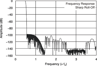 Figure 2. Amplitude vs Frequency
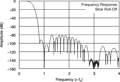 Figure 4. Amplitude vs Frequency
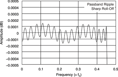 Figure 3. Amplitude vs Frequency
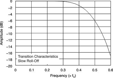 Figure 5. Amplitude vs Frequency
6.7.2 Digital Filter: De-Emphasis Filter
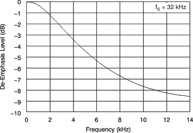 Figure 6. De-Emphasis Level vs Frequency
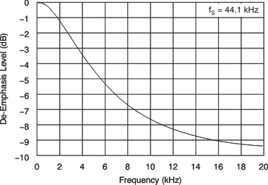 Figure 8. De-Emphasis Level vs Frequency
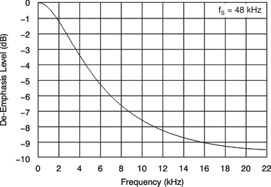 Figure 10. De-Emphasis Level vs Frequency
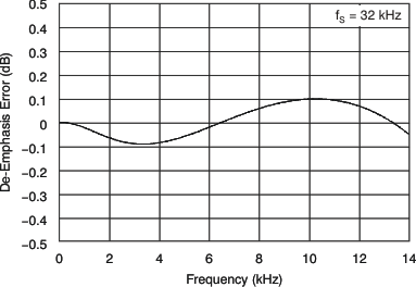 Figure 7. De-Emphasis Error vs Frequency
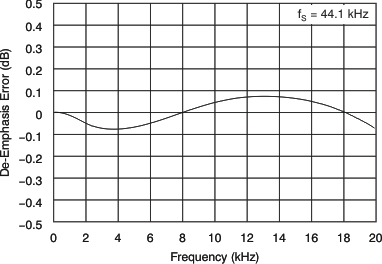 Figure 9. De-Emphasis Error vs Frequency
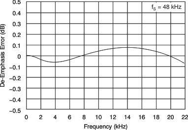 Figure 11. De-Emphasis Error vs Frequency
6.7.3 Analog Dynamic Performance: Supply Voltage Characteristics
PCM mode, TA = +25°C, and VDD = 3.3 V; measured with circuit shown in Figure 53, unless otherwise noted.
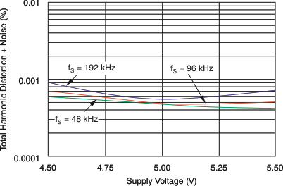 Figure 12. THD+N vs Supply Voltage
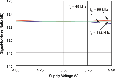 Figure 14. SNR vs Supply Voltage
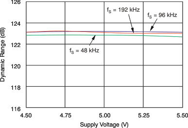 Figure 13. Dynamic Range vs Supply Voltage
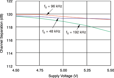 Figure 15. Channel Separation vs Supply Voltage
6.7.4 Analog Dynamic Performance: Temperature Characteristics
PCM mode, VDD = 3.3 V, and VCC = 5 V; measured with circuit shown in Figure 53, unless otherwise noted.
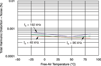 Figure 16. THD+N vs Free-Air Temperature
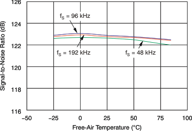 Figure 18. SNR vs Free-Air Temperature
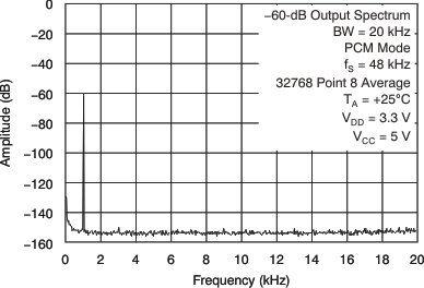 Figure 20. Amplitude vs Frequency
(Measurement Circuit: Figure 53)
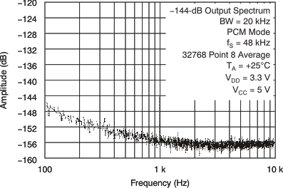 Figure 22. Amplitude vs Frequency
(Measurement Circuit: Figure 53)
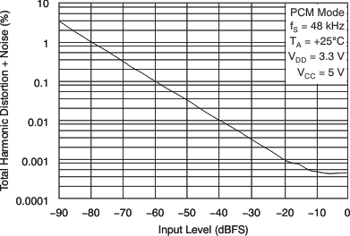 Figure 24. THD+N vs Input Level
(Measurement Circuit: Figure 53)
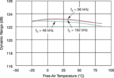 Figure 17. Dynamic Range vs Free-Air Temperature
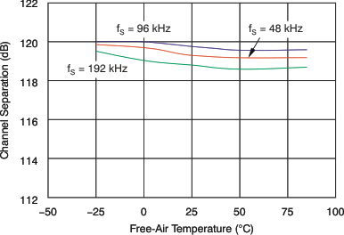 Figure 19. Channel Separation vs Free-Air Temperature
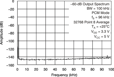 Figure 21. Amplitude vs Frequency
(Measurement Circuit: Figure 53)
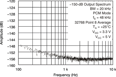 Figure 23. Amplitude vs Frequency
(Measurement Circuit: Figure 53)
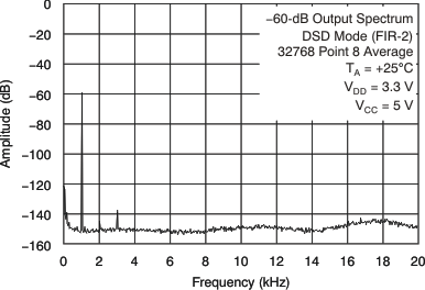 Figure 25. Amplitude vs Frequency
(Measurement Circuit: Figure 54)
6.7.5 Analog FIR Filter performance in DSD Mode
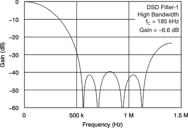
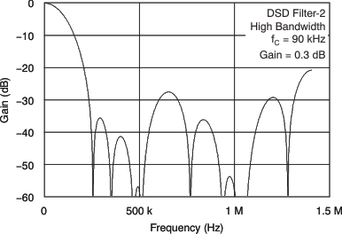
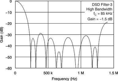
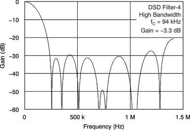
All specifications at DBCK = 2.8224 MHz (44.1 kHz × 64 fS), and 50% modulation DSD data input, unless otherwise noted.
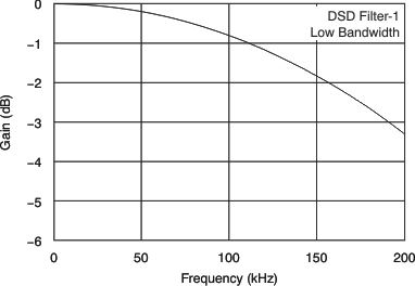 Figure 26. Gain vs Frequency
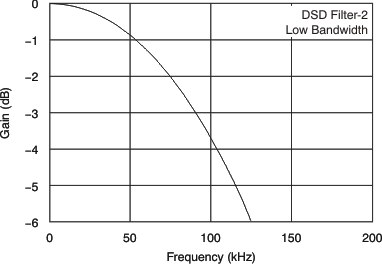 Figure 28. Gain vs Frequency
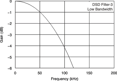 Figure 30. Gain vs Frequency
 Figure 32. Gain vs Frequency
