SLES177B April 2006 – August 2015 PCM1808
PRODUCTION DATA.
- 1 Features
- 2 Applications
- 3 Description
- 4 Revision History
- 5 Pin Configuration and Functions
- 6 Specifications
- 7 Detailed Description
- 8 Application and Implementation
- 9 Power Supply Recommendations
- 10Layout
- 11Device and Documentation Support
- 12Mechanical, Packaging, and Orderable Information
8 Application and Implementation
NOTE
Information in the following applications sections is not part of the TI component specification, and TI does not warrant its accuracy or completeness. TI’s customers are responsible for determining suitability of components for their purposes. Customers should validate and test their design implementation to confirm system functionality.
8.1 Application Information
The PCM1808 device is suitable for wide variety of cost-sensitive consumer applications requiring good performance and operation with a 5-V analog supply and 3.3-V digital supply.
8.2 Typical Application

8.2.1 Design Requirements
For this design example, use the parameters listed in Table 4 as the input parameters.
Table 4. Design Parameters
| DESIGN PARAMETER | EXAMPLE VALUE |
|---|---|
| Analog input voltage range | 0 Vp-p to 3 Vp-p |
| Output | PCM audio data |
| System clock input frequency | 2.048 MHz to 49.152 MHz |
| Output sampling frequency | 8 kHz to 96 kHz |
| Power supply | 3.3 V and 5 V |
8.2.2 Detailed Design Procedure
8.2.2.1 Control Pins
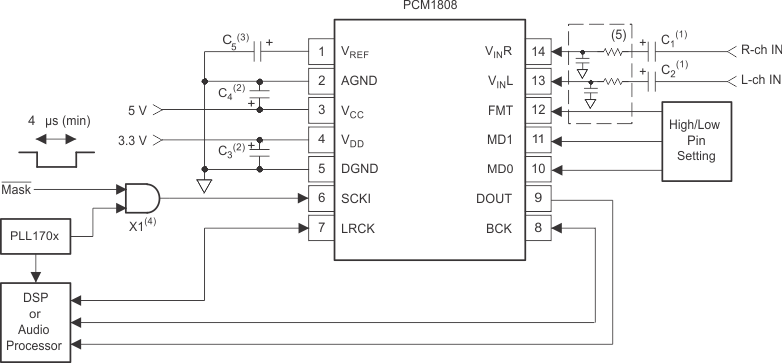
The control pins FMT, MD0, and MD1 should be controlled either by biasing with a 10 kΩ resister to VDD or GND, or by driving with GPIO from the DSP or audio processor.
8.2.2.2 Master Clock
In this application of the PCM1808 device, a PLL170X series device is used as the master clock source to drive both the PCM1808 and the DSP or audio processor synchronously. With the addition of the AND gate, the operation of the PCM1808 device can be halted by control of the MASK bit. A crystal that operates at the standard audio multiples can also be used.
8.2.2.3 DSP or Audio Processor
In this application, the DSP or audio processor is acting as the audio master, and the PCM1808 is acting as the audio slave. This means the DSP or audio processor must be able to output audio clocks that the PCM1808 can use to process audio signals.
8.2.2.4 Input Filters
For the analog input circuit, an ac coupling capacitor should be placed in series with the input. This will remove the dc component of the input signal. An RC filter can also be implemented to filter out-of-band noise to reduce aliasing. The equation below can be used to calculate the cutoff frequency of the optional RC filter for the input.

8.2.3 Application Curve
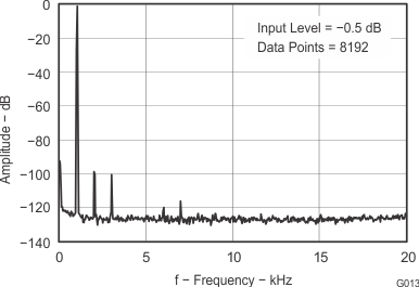
 Figure 27. Output Spectrum