SLES177B April 2006 – August 2015 PCM1808
PRODUCTION DATA.
- 1 Features
- 2 Applications
- 3 Description
- 4 Revision History
- 5 Pin Configuration and Functions
- 6 Specifications
- 7 Detailed Description
- 8 Application and Implementation
- 9 Power Supply Recommendations
- 10Layout
- 11Device and Documentation Support
- 12Mechanical, Packaging, and Orderable Information
6 Specifications
6.1 Absolute Maximum Ratings
over operating ambient temperature range (unless otherwise noted) (1)| MIN | MAX | UNIT | |||
|---|---|---|---|---|---|
| VCC | Analog supply voltage | –0.3 | 6.5 | V | |
| VDD | Digital supply voltage | –0.3 | 4 | V | |
| Ground voltage differences | AGND, DGND | ±0.1 | V | ||
| Digital input voltage | LRCK, BCK, DOUT | –0.3 | (VDD + 0.3 V) < 4 | V | |
| SCKI, MD0, MD1, FMT | –0.3 | 6.5 | V | ||
| VINL, VINR, VREF | Analog input voltage | –0.3 | (VCC + 0.3 V) < 6.5 | V | |
| Input current (any pins except supplies) | ±10 | mA | |||
| TJ | Junction temperature | 150 | °C | ||
| Tstg | Storage temperature | –55 | 150 | °C | |
(1) Stresses beyond those listed under Absolute Maximum Ratings may cause permanent damage to the device. These are stress ratings only, which do not imply functional operation of the device at these or any other conditions beyond those indicated under Recommended Operating Conditions. Exposure to absolute-maximum-rated conditions for extended periods may affect device reliability.
6.2 ESD Ratings
| VALUE | UNIT | |||
|---|---|---|---|---|
| V(ESD) | Electrostatic discharge | Human-body model (HBM), per ANSI/ESDA/JEDEC JS-001, all pins(1) | ±4000 | V |
| Charged-device model (CDM), per JEDEC specification JESD22-C101, all pins(2) | ±1500 | |||
(1) JEDEC document JEP155 states that 500-V HBM allows safe manufacturing with a standard ESD control process.
(2) JEDEC document JEP157 states that 250-V CDM allows safe manufacturing with a standard ESD control process.
6.3 Recommended Operating Conditions
over operating ambient temperature range (unless otherwise noted)| MIN | NOM | MAX | UNIT | |||
|---|---|---|---|---|---|---|
| VCC | Analog supply voltage (see Power Supply Recommendations) | 4.5 | 5 | 5.5 | V | |
| VDD | Digital supply voltage | 2.7 | 3.3 | 3.6 | V | |
| Analog input voltage, full scale (–0 dB) | VCC = 5 V | 3 | Vp-p | |||
| VIH (1) | High input logic level | 2 | VDD | VDC | ||
| VIL (1) | Low input logic level | 0 | 0.8 | VDC | ||
| VIH (2) (3) | High input logic level | 2 | 5.5 | VDC | ||
| VIL (2) (3) | Low input logic level | 0 | 0.8 | VDC | ||
| Digital input logic family | TTL compatible | |||||
| Digital input clock frequency, system clock | 2.048 | 49.152 | MHz | |||
| Digital input clock frequency, sampling clock | 8 | 96 | kHz | |||
| Digital output load capacitance | 20 | pF | ||||
| TA | Operating ambient temperature range | –40 | 85 | °C | ||
| TJ | Junction temperature | 150 | °C | |||
(1) Pins 7, 8: LRCK, BCK (Schmitt-trigger input, with 50-kΩ typical pulldown resistor, in slave mode)
(2) Pin 6: SCKI (Schmitt-trigger input, 5-V tolerant)
(3) Pins 10–12: MD0, MD1, FMT (Schmitt-trigger input, with 50-kΩ typical pulldown resistor, 5-V tolerant)
6.4 Thermal Information
| THERMAL METRIC(1) | PCM1808 | UNIT | |
|---|---|---|---|
| PW (TSSOP) | |||
| 14 PINS | |||
| RθJA | Junction-to-ambient thermal resistance | 89.4 | °C/W |
| RθJC(top) | Junction-to-case (top) thermal resistance | 25.6 | °C/W |
| RθJB | Junction-to-board thermal resistance | 30.3 | °C/W |
| ψJT | Junction-to-top characterization parameter | 1.4 | °C/W |
| ψJB | Junction-to-board characterization parameter | 29.8 | °C/W |
| RθJC(bot) | Junction-to-case (bottom) thermal resistance | N/A | °C/W |
(1) For more information about traditional and new thermal metrics, see the Semiconductor and IC Package Thermal Metrics application report, SPRA953.
6.5 Electrical Characteristics
All specifications at TA = 25°C, VCC = 5 V, VDD = 3.3 V, master mode, fS = 48 kHz, system clock = 512 fS, 24-bit data, unless otherwise noted| PARAMETER | TEST CONDITIONS | MIN | TYP | MAX | UNIT | |
|---|---|---|---|---|---|---|
| Resolution | 24 | Bits | ||||
| DATA FORMAT | ||||||
| Audio data interface format | I2S, left-justified | |||||
| Audio data bit length | 24 | Bits | ||||
| Audio data format | MSB-first, 2s complement | |||||
| fS | Sampling frequency | 8 | 48 | 96 | kHz | |
| System clock frequency | 256 fS | 2.048 | 12.288 | 24.576 | MHz | |
| 384 fS | 3.072 | 18.432 | 36.864 | |||
| 512 fS | 4.096 | 24.576 | 49.152 | |||
| INPUT LOGIC | ||||||
| VIH (1) | High input logic level | 2 | VDD | VDC | ||
| VIL (1) | Low input logic level | 0 | 0.8 | VDC | ||
| VIH (2) (3) | High input logic level | 2 | 5.5 | VDC | ||
| VIL (2) (3) | Low input logic level | 0 | 0.8 | VDC | ||
| IIH (2) | High input logic current | VIN = VDD | ±10 | µA | ||
| IIL (2) | Low input logic current | VIN = 0 V | ±10 | µA | ||
| IIH (1) (3) | High input logic current | VIN = VDD | 65 | 100 | µA | |
| IIL (1) (3) | Low input logic current | VIN = 0 V | ±10 | µA | ||
| OUTPUT LOGIC | ||||||
| VOH (4) | High output logic level | IOUT = –4 mA | 2.8 | VDC | ||
| VOL (4) | Low output logic level | IOUT = 4 mA | 0.5 | VDC | ||
| DC ACCURACY | ||||||
| Gain mismatch, channel-to-channel | ±1 | ±3 | % of FSR | |||
| Gain error | ±3 | ±6 | % of FSR | |||
| DYNAMIC PERFORMANCE (5) | ||||||
| THD+N | Total harmonic distortion + noise | VIN = –0.5 dB, fS = 48 kHz | –93 | –87 | dB | |
| VIN = –0.5 dB, fS = 96 kHz (6) | –87 | |||||
| VIN = –60 dB, fS = 48 kHz | –37 | |||||
| VIN = –60 dB, fS = 96 kHz (6) | –39 | |||||
| Dynamic range | fS = 48 kHz, A-weighted | 95 | 99 | dBVDC | ||
| fS = 96 kHz, A-weighted (6) | 101 | |||||
| S/N | Signal-to-noise ratio | fS = 48 kHz, A-weighted | 95 | 99 | dB | |
| fS = 96 kHz, A-weighted (6) | 101 | |||||
| Channel separation | fS = 48 kHz | 93 | 97 | dB | ||
| fS = 96 kHz (6) | 91 | |||||
| ANALOG INPUT | ||||||
| Input voltage | 0.6 VCC | Vp-p | ||||
| Center voltage (VREF) | 0.5 VCC | V | ||||
| Input impedance | 60 | kΩ | ||||
| Antialiasing filter frequency response | –3 dB | 1.3 | MHz | |||
| DIGITAL FILTER PERFORMANCE | ||||||
| Pass band | 0.454 fS | Hz | ||||
| Stop band | 0.583 fS | Hz | ||||
| Pass-band ripple | ±0.05 | dB | ||||
| Stop-band attenuation | –65 | dB | ||||
| Delay time | 17.4 / fS | |||||
| HPF frequency response | –3 dB | 0.019 fS / 1000 | ||||
| POWER SUPPLY REQUIREMENTS | ||||||
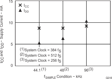
| ICC | Analog supply current (7) | fS = 48 kHz, 96 kHz (6) | 8.6 | 11 | mA | |
| Powered down (8) | 1 | μA | ||||
| IDD | Digital supply current (7) | fS = 48 kHz | 5.9 | 8 | mA | |
| fS = 96 kHz (6) | 10.2 | mA | ||||
| Powered down (8) | 150 | µA | ||||
| Power dissipation (7) | fS = 48 kHz | 62 | 81 | mW | ||
| fS = 96 kHz (6) | 77 | |||||
| Powered down (8) | 500 | µW | ||||
(1) Pins 7, 8: LRCK, BCK (Schmitt-trigger input, with 50-kΩ typical pulldown resistor, in slave mode)
(2) Pin 6: SCKI (Schmitt-trigger input, 5-V tolerant)
(3) Pins 10–12: MD0, MD1, FMT (Schmitt-trigger input, with 50-kΩ typical pulldown resistor, 5-V tolerant)
(4) Pins 7–9: LRCK, BCK (in master mode), DOUT
(5) Testing of analog performance specifications uses an audio measurement system by Audio Precision™ with 400-Hz HPF and 20-kHz LPF in RMS mode.
(6) fS = 96 kHz, system clock = 256 fS.
(7) Minimum load on LRCK (pin 7), BCK (pin 8), DOUT (pin 9)
(8) Power-down and reset functions enabled by halting SCKI, BCK, LRCK.
6.6 Timing Requirements
| MIN | NOM | MAX | UNIT | ||
|---|---|---|---|---|---|
| SYSTEM CLOCK TIMING | |||||
| tw(SCKH) | System clock pulse duration, HIGH | 8 | ns | ||
| tw(SCKL) | System clock pulse duration, LOW | 8 | ns | ||
| System clock duty cycle | 40% | 60% | |||
| CLOCK-HALT POWER-DOWN AND RESET TIMING | |||||
| t(CKR) | Delay time from SCKI halt to internal reset | 4 | µs | ||
| t(RST) | Delay time from SCKI resume to reset release | 1024 SCKI | µs | ||
| t(REL) | Delay time from reset release to DOUT output | 8960 / fS | µs | ||
| AUDIO DATA INTERFACE TIMING (Slave Mode: LRCK and BCK Work as Inputs)(1) | |||||
| t(BCKP) | BCK period | 1 / (64 fS) | ns | ||
| t(BCKH) | BCK pulse duration, HIGH | 1.5 × t(SCKI) | ns | ||
| t(BCKL) | BCK pulse duration, LOW | 1.5 × t(SCKI) | ns | ||
| t(LRSU) | LRCK setup time to BCK rising edge | 50 | ns | ||
| t(LRHD) | LRCK hold time to BCK rising edge | 10 | ns | ||
| t(LRCP) | LRCH period | 10 | µs | ||
| t(CKDO) | Delay time, BCK falling edge to DOUT valid | –10 | 40 | ns | |
| t(LRDO) | Delay time, LRCK edge to DOUT valid | –10 | 40 | ns | |
| tr | Rise time of all signals | 20 | ns | ||
| tf | Fall time of all signals | 20 | ns | ||
| AUDIO DATA INTERFACE TIMING (Master Mode: LRCK and BCK Work as Outputs)(2) | |||||
| t(BCKP) | BCK period | 150 | 1 / (64 fS) | 2000 | ns |
| t(BCKH) | BCK pulse duration, HIGH | 65 | 1200 | ns | |
| t(BCKL) | BCK pulse duration, LOW | 65 | 1200 | ns | |
| t(CKLR) | Delay time, BCK falling edge to LRCK valid | –10 | 20 | ns | |
| t(LRCP) | LRCK period | 10 | 1 / fS | 125 | ns |
| t(CKDO) | Delay time, BCK falling edge to DOUT valid | –10 | 20 | ns | |
| t(LRDO) | Delay time, LRCK edge to DOUT valid | –10 | 20 | ns | |
| tr | Rise time of all signals | 20 | ns | ||
| tf | Fall time of all signals | 20 | ns | ||
| AUDIO CLOCK INTERFACE TIMING (Master Mode: BCK Work as Outputs)(3) | |||||
| t(SCKBCK) | Delay time, SCKI rising edge to BCK edge | 5 | 30 | ns | |
(1) Timing measurement reference level is 1.4 V for input and 0.5 VDD for output. Rise and fall times are from 10% to 90% of the input-output signal swing. Load capacitance of DOUT is 20 pF. t(SCKI) is the SCKI period.
(2) Timing measurement reference level is 0.5 VDD. Rise and fall times are from 10% to 90% of the input-output signal swing. Load capacitance of all signals is 20 pF.
(3) Timing measurement reference level is 1.4 V for input and 0.5 VDD for output. Load capacitance of BCK is 20 pF. This timing applies when SCKI frequency is less than 25 MHz.
 Figure 1. System Clock Timing
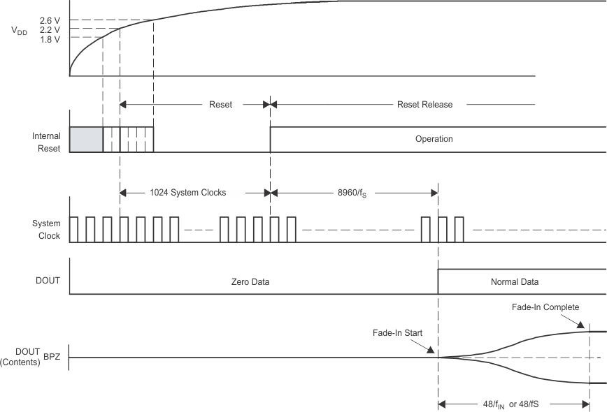 Figure 2. Power-On Timing
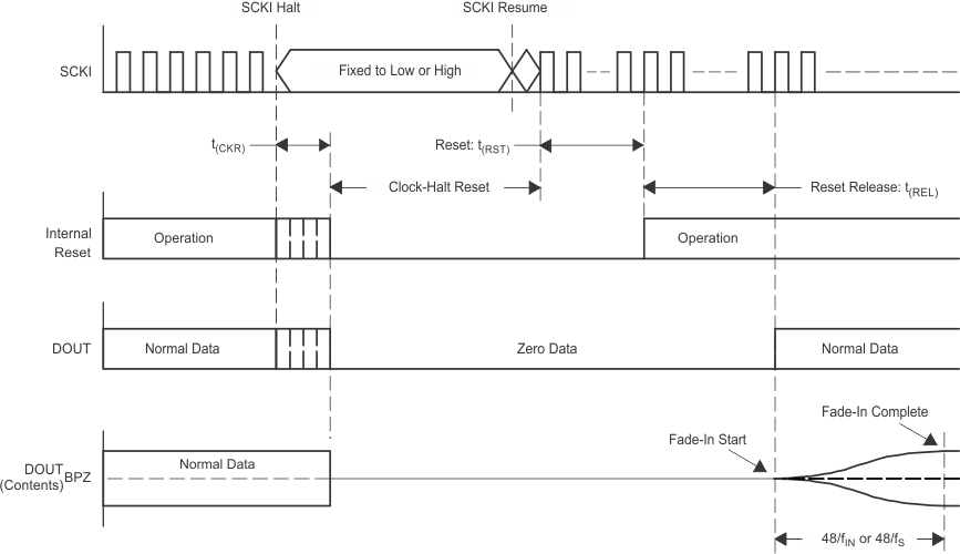 Figure 3. Clock-Halt Power-Down and Reset Timing
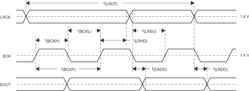 Figure 4. Audio Data Interface Timing (Slave Mode: LRCK and BCK Work as Inputs)
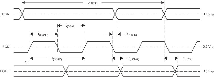 Figure 5. Audio Data Interface Timing (Master Mode: LRCK and BCK Work as Outputs)
 Figure 6. Audio Clock Interface Timing (Master Mode: BCK Works as Output)
6.7 Typical Characteristics
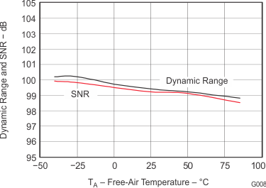
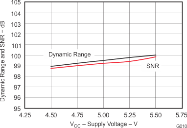
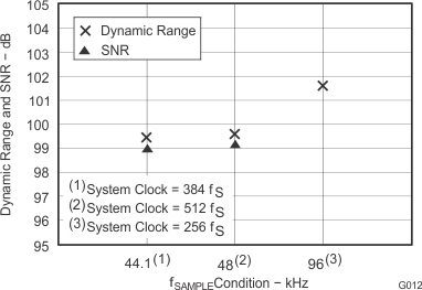
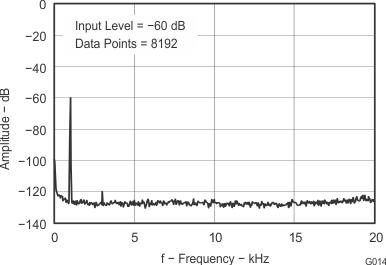
All specifications at TA = 25°C, VCC = 5 V, VDD = 3.3 V, master mode, fS = 48 kHz, system clock = 512 fS, 24-bit data, unless otherwise noted.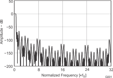
Overall Characteristics
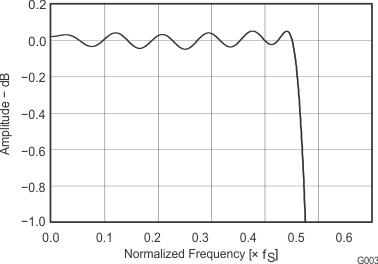
Pass-Band Ripple Characteristics
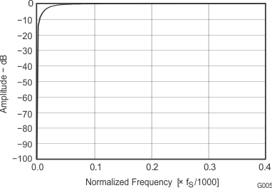
HPF Stop-Band Characteristics
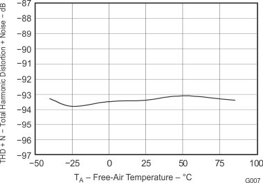
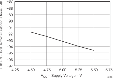
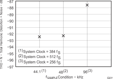
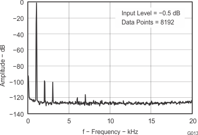
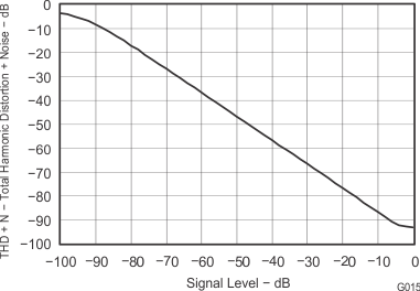
THD+N vs Signal Level
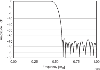
Stop-Band Attenuation Characteristics
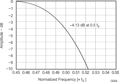
Transition-Band Characteristics
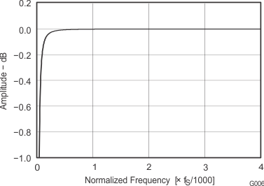
HPF Stop-Band Characteristics
