SBFS036B May 2015 – August 2015 PCM2704C , PCM2705C , PCM2706C
PRODUCTION DATA.
- 1 Features
- 2 Applications
- 3 Description
- 4 Revision History
- 5 Device Comparison Table
- 6 Pin Configuration and Functions
-
7 Specifications
- 7.1 Absolute Maximum Ratings
- 7.2 ESD Ratings
- 7.3 Recommended Operating Conditions
- 7.4 Thermal Information: PCM2704C, PCM2705C
- 7.5 Thermal Information: PCM2706C, PCM2707C
- 7.6 Electrical Characteristics: PCM2704CDB, PCM2705CDB, PCM2706CPJT, PCM2707CPJT
- 7.7 Audio Interface Timing Characteristics
- 7.8 Audio Clock Timing Characteristics
- 7.9 External ROM Read Interface Timing Characteristics
- 7.10 SPI Timing Characteristics
- 7.11 Typical Characteristics
- 8 Parameter Measurement Information
-
9 Detailed Description
- 9.1 Overview
- 9.2 Functional Block Diagrams
- 9.3
Feature Description
- 9.3.1 Clock and Reset
- 9.3.2 Operation Mode Selection
- 9.3.3 DAC
- 9.3.4 Digital Audio Interface: S/PDIF Output
- 9.3.5 Digital Audio Interface: I2S Interface Output (PCM2706C/7C)
- 9.3.6 Descriptor Data Modification
- 9.3.7 External ROM Descriptor (PCM2704C/6C)
- 9.3.8 External ROM Example
- 9.3.9 Serial Programming Interface (PCM2705C/7C)
- 9.3.10 USB Host Interface Sequence
- 9.3.11 Operating Environment
- 9.4 Device Functional Modes
- 9.5 Programming
- 9.6 Register Maps
- 10Application and Implementation
- 11Power Supply Recommendations
- 12Layout
- 13Device and Documentation Support
- 14Mechanical, Packaging, and Orderable Information
9 Detailed Description
9.1 Overview
The PCM2704C/5C/6C/7C is a stereo audio digital-to-analog converter (DAC) with USB connection capability and a S/PDIF digital interface.
The PCM2704C/5C/6C/7C can be used in self-powered and bus-powered modes. These devices meet the requirements of USB2.0 standard connection. The PCM2704C/5C/6C/7C has digital input from the USB port. The PCM2704C/5C provides two different paths for the audio data, one of which goes to the digital S/PDIF output, and the other to the analog output through the DAC. The PCM2706C/7C provides three different paths for the audio data; to the digital S/PDIF output, to the analog output through the DAC, and leading the audio data to the I2S digital output (the I2S path is selectable trough FSEL pin 9).
The PCM2704C has 3 external interrupts (HID) which control the Mute, Volume Up, and Volume Down; these control inputs are active High. The PCM2706C has 7 external interrupts (I2S/HID control is selectable trough FSEL pin 9) which control the Mute, Volume Up, Volume Down, Next track, Previous track, Play/Pause, and Stop; these control inputs are active High. The PCM2704C/5C/6C/7C requires a 12-MHz clock, which can be provided by an external clock or generated by a built-in crystal resonator.
9.2 Functional Block Diagrams
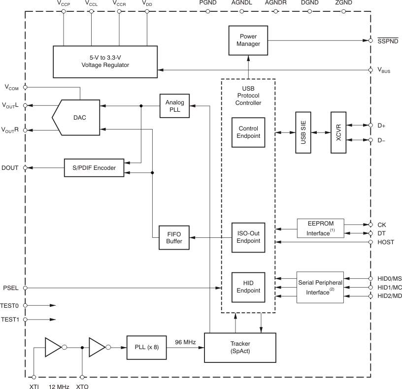

9.3 Feature Description
9.3.1 Clock and Reset
For both USB and audio functions, the PCM2704C/5C/6C/7C require a 12-MHz (±500 ppm) clock that can be generated by the onboard oscillator using a 12-MHz crystal resonator. The 12-MHz crystal resonator must be connected to the XTI pin (pin 28 for the PCM2704C/5C, pin 12 for the PCM2706C/7C) and the XTO pin (pin 1 for the PCM2704C/5C, pin 13 for the PCM2706C/7C) with one large (1-MΩ) resistor and two small capacitors; the capacitance of these components depends on the specified load capacitance of the crystal resonator. An external clock can be supplied from XTI (pin 28 for the PCM2704C/5C, pin 12 for the PCM2706C/7C). If an external clock is supplied, XTO (pin 1 for the PCM2704C/5C, pin 13 for the PCM2706C/7C) must be left open. No clock disabling pin is provided; therefore, TI does not recommend to use the external clock supply. SSPND (pin 27 for the PCM2704C/5C, pin 11 for the PCM2706C/7C) cannot use clock disabling.
The PCM2704C/5C/6C/7C have an internal power-on reset circuit, which works automatically when VDD (pin 7 for the PCM2704C/5C, pin 21 for the PCM2706C/7C) exceeds 2-V typical (1.6 to 2.4 V), which is equivalent to VBUS (pin 10 for the PCM2704C/5C, pin 24 for the PCM2706C/7C) exceeding 3-V typical for bus-powered applications. Approximately 700 μs is required until an internal reset release occurs.
9.3.2 Operation Mode Selection
The PCM2704C/5C/6C/7C have the following mode-select pins.
9.3.2.1 Power Configuration Select/Host Detection
PSEL (pin 4 for the PCM2704C/5C, pin 16 for the PCM2706C/7C) is dedicated to selecting the power source. This selection affects the configuration descriptor. While in bus-powered operation, the maximum power consumption from VBUS is determined by the HOST pin (pin 21 for the PCM2704C/5C, pin 3 for the PCM2706C/7C). For self-powered operation, the HOST pin must be connected to VBUS of the USB bus with a pulldown resistor to detect attach and detach. (To avoid excessive suspend current, the pulldown should be a high-value resistor.) Table 1 summarizes the power configuration select options.
Table 1. Power Configuration Select
| PSEL | DESCRIPTION |
|---|---|
| 0 | Self-powered |
| 1 | Bus-powered |
| HOST | DESCRIPTION |
| 0 | Detached from USB (self-powered)/100 mA (bus-powered) |
| 1 | Attached to USB (self-powered)/500 mA (bus-powered) |
9.3.2.2 Function Select (PCM2706C/7C Only)
FSEL (pin 9) determines the function of the FUNC0 through FUNC3 pins (pins 4, 5, 18, and 19) and DOUT (pin 17). When the I2S interface is required, FSEL must be low. Otherwise, FSEL must be high. Table 2 lists the functionality of the FUNC0 through FUNC3 pins, based on the FSEL pin.
9.3.3 DAC
The PCM2704C/5C/6C/7C have a DAC that uses an oversampling technique with 128-ƒS, second-order, multi-bit noise shaping. This technique provides extremely-low quantization noise in the audio band, and the built-in analog low-pass filter removes the high-frequency components of the noise-shaping signal. The DAC analog outputs, VOUTL and VOUTR , are sent through the headphone amplifier and can provide 12 mW at 32 Ω as well as 1.8 VPP into a 10-kΩ load.
9.3.4 Digital Audio Interface: S/PDIF Output
The PCM2704C/5C/6C/7C employ S/PDIF output. Isochronous-out data from the host are encoded to S/PDIF output DOUT, as well as to DAC analog outputs VOUTL and VOUTR. The interface format and timing follow the IEC-60958 standard. Monaural data are converted to the stereo format at the same data rate. S/PDIF output is not supported in the I2S I/F enable mode. The implementation of this feature is optional.
NOTE
It is the responsibility of the user to determine whether or not to implement this feature in the end application.
9.3.4.1 Channel Status Information
Channel status information is fixed, and includes consumer application, PCM mode, copyright, and digital/digital converter data. All other bits are fixed as 0s, except for the sample frequency, which is set automatically according to the data received through the USB.
9.3.4.2 Copyright Management
Digital audio data output is always encoded as original with SCMS control. Only one generation of digital duplication is allowed.
9.3.5 Digital Audio Interface: I2S Interface Output (PCM2706C/7C)
The PCM2706C and PCM2707C can support the I2S interface, which is enabled by the FSEL pin (pin 9). In the I2S interface-enabled mode, pins 4, 18, 19, 5, and 17 are assigned as DIN, SYSCK, BCK, LRCK, and DOUT, respectively. These pins provide digital output/input data in the 16-bit I2S format, which is also accepted by the internal DAC. Figure 1, Figure 2, and Figure 3 show the I2S interface format and timing. Audio Interface Timing Characteristics and Audio Clock Timing Characteristics list the audio interface timing and audio clock timing characteristics, respectively.
9.3.6 Descriptor Data Modification
The descriptor data can be modified through the I2C port by external ROM (PCM2704C/6C) or through the SPI port by an SPI host such as an MCU (PCM2705C/7C) under a particular configuration of the PSEL and HOST pins. Setting both the PSEL and the HOST pins high is necessary to modify the descriptor data; the D+ pin pullup resistor must not be activated before programming the descriptor data through the external ROM or SPI port is completed. The descriptor data must be sent from an external ROM to the PCM2704C/6C or from the SPI host to the PCM2705C/7C in LSB first format, with a specified byte order. Additionally, the power attribute and max power contents must be consistent with the PSEL setting and the power usage from the USB VBUS of the end application. Therefore, the device does not support descriptor data modification in self-powered configuration (PSEL = low).
9.3.7 External ROM Descriptor (PCM2704C/6C)
The PCM2704C/6C support an external ROM interface to override internal descriptors. Pin 3 (for the PCM2704C) or pin 15 (for the PCM2706C) is assigned as DT (serial data), and pin 2 (for the PCM2704C) or pin 14 (for the PCM2706C) is assigned as CK (serial clock) of the I2C interface when using the external ROM descriptor. Descriptor data are transferred from the external ROM to the PCM2704C/6C through the I2C interface the first time when the device is activated after a power-on reset. Before completing a read of the external ROM, the PCM2704C/6C reply with NACK for any USB command request from the host to the device itself. The descriptor data, which can be in the external ROM, must meet these parameters:
- String descriptors must be described in ANSI ASCII code (1 byte for each character).
- String descriptors are converted automatically to unicode strings for transmission to the host.
- The device address of the external ROM is fixed as 0xA0.
The data bits must be sent from LSB to MSB on the I2C bus. This condition means that each byte of data must be stored with its bits in reverse order. A read operation is performed at a frequency of XTI/384 (approximately 30 kHz). The power attribute and max power contents must be consistent with the end application circuit configuration (the PSEL setting and the actual power usage from VBUS of the USB connector); otherwise, it may cause improper or unexpected PCM2704C/6C operation.
The data must be stored from address 0x00 and must consist of 57 bytes, according to these listed parameters:
- Vendor ID (2 bytes)
- Product ID (2 bytes)
- Product string (16 bytes in ANSI ASCII code)
- Vendor string (32 bytes in ANSI ASCII code)
- Power attribute (1 byte)
- Max power (1 byte)
- Auxiliary HID usage ID in report descriptor (3 bytes)
Figure 28 shows the timing for an external ROM read operation. Table 3 summarizes the timing characteristics.
 Figure 28. External ROM Read Operation
Table 3. External ROM Read Operation Characteristics
| M | M | M | S | S | M | S | M | S | M | M |
|---|---|---|---|---|---|---|---|---|---|---|
| S | Device address | R/W | ACK | DATA | ACK | DATA | ACK | . . . | NACK | P |
9.3.8 External ROM Example
External ROM data (sample set)
0xBB, 0x08, 0x04, 0x27,
 0x50, 0x72, 0x6F, 0x64, 0x75, 0x63, 0x74, 0x20, 0x73, 0x74, 0x72, 0x69, 0x6E, 0x67, 0x73, 0x2E,
 0x56, 0x65, 0x6E, 0x64, 0x6F, 0x72, 0x20, 0x73, 0x74, 0x72, 0x69, 0x6E, 0x67, 0x73, 0x20, 0x61,
 0x72, 0x65, 0x20, 0x70, 0x6C, 0x61, 0x63, 0x65, 0x64, 0x20, 0x68, 0x65, 0x72, 0x65, 0x2E, 0x20,
 0x80,
 0x7D,
 0x0A, 0x93, 0x01
Explanation
Data are stored beginning at address 0x00
Vendor ID: 0x08BB
Product ID: 0x2704
Product string: Product strings (16 bytes)
Vendor string: Vendor strings are placed here (32 bytes, 31 visible characters are followed by 1 space).
Power attribute (bmAttribute): 0x80 (bus-powered)
Max power (maxPower): 0x7D (250 mA)
Auxiliary HID usage ID: 0x0A, 0x93, 0x01 (AL A/V capture)
Note that the data bits must be sent from LSB to MSB on the I2C bus. Therefore, each data byte must be stored with its bits in reverse order.
9.3.9 Serial Programming Interface (PCM2705C/7C)
The PCM2705C/7C supports a SPI to program the descriptor and to set the HID state. External ROM Descriptor (PCM2704C/6C) describes descriptor data. Figure 5 shows the SPI timing; SPI Timing Characteristics lists the respective timing characteristics.
Figure 29 shows the SPI write timing sequence.
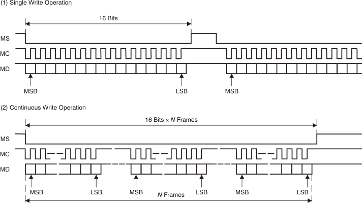 Figure 29. SPI Write Operation
9.3.10 USB Host Interface Sequence
9.3.10.1 Power-On, Attach, and Playback Sequence
The PCM2704C/5C/6C/7C are ready for setup when the reset sequence has finished and the USB bus is attached. After a connection has been established (through the setup process), the PCM2704C/5C/6C/7C are ready to accept USB audio data. While waiting for the audio data (that is, the device is in an idle state), the analog output is set to bipolar zero (BPZ).
Upon receiving the audio data, the PCM2704C/5C/6C/7C stores the first audio packet in the internal storage buffer. The packet contains 1 ms of audio data. The PCM2704C/5C/6C/7C start playing the audio data after detecting the next subsequent start-of-frame (SOF) packet. Figure 30 shows the initial operation sequence for the device.
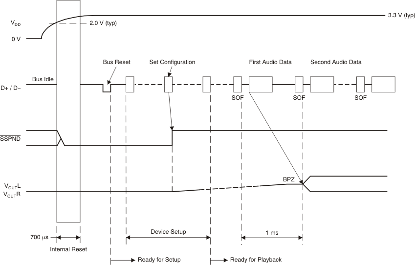 Figure 30. Initial Sequence
9.3.10.2 Play, Stop, and Detach Sequence
When the host finishes or aborts playback, the PCM2704C/5C/6C/7C stop playing after the last audio data output is complete. Figure 31 shows the play, stop, and detach sequence.
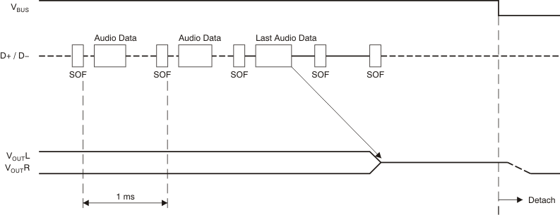 Figure 31. Play, Stop, and Detach Sequence
9.3.10.3 Suspend and Resume Sequence
The PCM2704C/5C/6C/7C enter a suspended state after the USB bus has been in a constant idle state for approximately 5 ms. While the PCM2704C/5C/6C/7C are in this suspended state, the SSPND flag (pin 27 for the PCM2704C/5C, pin 11 for the PCM2706C/7C) is asserted. The PCM2704C/5C/6C/7C wake up immediately when detecting a non-idle state on the USB bus. Figure 32 shows the operating sequence for the suspend and resume process.
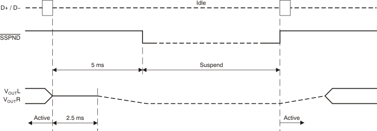 Figure 32. Suspend and Resume
9.3.11 Operating Environment
For current information on the PCM2704C/2705C/2706C/2707C operating environments, see the Updated Operating Environments for PCM270X, PCM290X Applications application report, SLAA374, available through the TI website at www.ti.com.
9.4 Device Functional Modes
The PCM2903C is a USB-controlled device. The PCM2903C is a digital-to-analog converter (DAC), with digital input (that goes to a D/A converter) and analog output, alongside the digital path to USB and S/PDIF and I2S (only in PCM2706C/7C). A wider explanation of these operational modes is shown in Feature Description.
9.5 Programming
9.5.1 USB Interface
Control data and audio data are transferred to the PCM2704C/5C/6C/7C through the D+ pin (pin 9 for the PCM2704C/5C, pin 23 for the PCM2706C/7C) and D– pin (pin 8 for the PCM2704C/5C, pin 22 for the PCM2706C/7C). D+ should be pulled up with a 1.5-kΩ (±5%) resistor. To avoid back voltage in self-powered operation, the device must not provide power to the pullup resistor on D+ while VBUS of the USB port is inactive.
All data to/from the PCM2704C/5C/6C/7C are transferred at full speed. Table 4 shows the information that is provided in the device descriptor. Some parts of the device descriptor can be modified through external ROM (PCM2704C/6C) or SPI (PCM2705C/7C).
Table 4. Device Descriptor
| DEVICE DESCRIPTOR | DESCRIPTION |
|---|---|
| USB revision | 1.1 compliant |
| Device class | 0x00 (device defined interface level) |
| Device subclass | 0x00 (not specified) |
| Device protocol | 0x00 (not specified) |
| Max packet size for endpoint 0 | 8 bytes |
| Vendor ID | 0x08BB (default value, can be modified) |
| Product ID | 0x27C4/0x27C5/0x27C6/0x27C7 (These values correspond to the model number, and the value can be modified.) |
| Device release number | 1.0 (0x0100) |
| Number of configurations | 1 |
| Vendor strings | BurrBrown from Texas Instruments (default value, can be modified) |
| Product strings | USB AUDIO DAC (default value, can be modified) |
| Serial number | Not supported |
Table 5 shows the information contained in the configuration descriptor. Some parts of the configuration descriptor can be modified through external ROM (PCM2704C/6C) or SPI (PCM2705C/7C).
Table 5. Configuration Descriptor
| CONFIGURATION DESCRIPTOR | DESCRIPTION |
|---|---|
| Interface | Three interfaces |
| Power attribute | 0x80 or 0xC0 (bus-powered or self-powered, depending on PSEL; no remote wake up. This value can be modified.) |
| Max power | 0x0A, 0x32, or 0xFA (20 mA for self-powered, 100 mA or 500 mA for bus-powered, depending on PSEL and HOST. This value can be modified.) |
Table 6 shows the information contained in the string descriptor. Some parts of the string descriptor can be modified through external ROM (PCM2704C/6C) or SPI (PCM2705C/7C).
Table 6. String Descriptor
| STRING DESCRIPTOR | DESCRIPTION |
|---|---|
| 0 | 0x0409 |
| 1 | BurrBrown from Texas Instruments (default value, can be modified) |
| 2 | USB AUDIO DAC (default value, can be modified) |
9.5.1.1 Device Configuration
Figure 33 shows the USB audio function topology. The PCM2704C/5C/6C/7C have three interfaces. Each interface is enabled by different alternative settings.
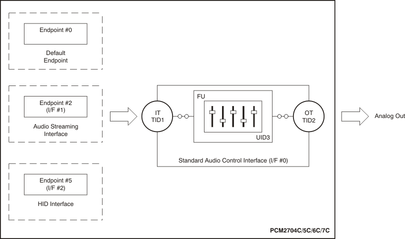 Figure 33. USB Audio Function Topology
9.5.1.2 Interface Number 0 (Default/Control Interface)
Interface number 0 is the control interface. Setting number 0 is the only possible setting for interface number 0. Setting number 0 describes the standard audio control interface. The audio control interface consists of a terminal. The PCM2704C/5C/6C/7C have three terminals:
- Input terminal (IT number 1) for isochronous-out stream
- Output terminal (OT number 2) for audio analog output
- Feature unit (FU number 3) for DAC digital attenuator
Input terminal number 1 is defined as a USB stream (terminal type 0x0101). Input terminal number 1 can accept two-channel audio streams consisting of left and right channels. Output terminal number 2 is defined as a speaker (terminal type 0x0301). Feature unit number 3 supports these sound control features:
- Volume control
- Mute control
The built-in digital volume controller can be manipulated by an audio-class-specific request from 0 to –64 dB in steps of 1 dB. Changes are made by incrementing or decrementing one step (that is, 1 dB) for every 1 / ƒS time interval, until the volume level reaches the requested value. Each channel can be set to a separate value. The master volume control is not supported. A request to the master volume is stalled and ignored. The built-in digital mute controller can be manipulated by an audio-class-specific request. A master mute control request is acceptable. A mute control request to an individual channel is stalled and ignored. The digital volume control does not affect either the S/PDIF or I2S outputs (PCM2706C/7C only).
9.5.1.3 Interface Number 1 (Isochronous-Out Interface)
Interface number 1 is for the audio-streaming data-out interface. Interface number 1 has the alternative settings described in Table 7. Alternative setting number 0 is the zero-bandwidth setting. All other alternative settings are operational settings.
Table 7. Interface Number 1 Parameters
| ALTERNATIVE SETTING | DATA FORMAT | TRANSFER MODE | SAMPLING RATE (kHz) |
||
|---|---|---|---|---|---|
| 00 | Zero bandwidth | ||||
| 01 | 16-bit | Stereo | 2's complement (PCM) | Adaptive | 32, 44.1, 48 |
| 02 | 16-bit | Mono | 2's complement (PCM) | Adaptive | 32, 44.1, 48 |
9.5.1.4 Interface Number 2 (HID Interface)
Interface number 2 is the interrupt-data-in interface. The HID consumer control device consists of interface number 2. Alternative setting number 0 is the only possible setting for interface number 2.
On the HID device descriptor, eight HID items are reported for any model, in any configuration.
9.5.1.4.1 HID Items Reported
9.5.1.4.1.1 Basic HID Operation
Interface number 2 can report these three key statuses for any model. These statuses can be set by the HID0 through HID2 pins (PCM2704C/6C) or the SPI port (PCM2705C/7C).
- Mute (0xE2)
- Volume up (0xE9)
- Volume down (0xEA)
9.5.1.4.1.2 Extended HID Operation (PCM2705/6/7)
By using the FUNC0 through FUNC3 pins (PCM2706C) or the SPI port (PCM2705C/7C), these additional conditions can be reported to the host.
- Play/Pause (0xCD)
- Stop (0xB7)
- Previous (0xB6)
- Next (0xB5)
9.5.1.4.1.3 Auxiliary HID Status Report (PCM2705C/7C)
One additional HID status can be reported to the host though the SPI port. This status flag is defined by SPI command or external ROM. This definition must be described as on the report descriptor with a three-byte usage ID. AL A/V Capture (0x0193) is assigned as the default value for this status flag.
9.5.1.5 Endpoints
The PCM2704C/5C/6C/7C has three endpoints:
- Control endpoint (EP number 0)
- Isochronous-out audio data-stream endpoint (EP number 2)
- HID endpoint (EP number 5)
The control endpoint is a default endpoint. The control endpoint controls all functions of the PCM2704C/5C/6C/7C by standard USB request and USB audio-class-specific request from the host. The isochronous-out audio data-stream endpoint is an audio sink endpoint that receives the PCM audio data. The isochronous-out audio data-stream endpoint accepts the adaptive transfer mode. The HID endpoint is an interrupt-in endpoint. The HID endpoint reports HID status every 10 ms.
The HID endpoint is defined as a consumer-control device. The HID function is designed as an independent endpoint from the isochronous-out endpoint. This configuration means that the effect of HID operation depends on the host software. Typically, the HID function controls the primary audio-out device.
9.6 Register Maps
9.6.1 SPI Register (PCM2705C/7C)
NOTE
Contents of the power attribute and max power must be consistent with the actual application circuit configuration (the PSEL setting and the actual power usage from VBUS of the USB connector); otherwise, it may cause improper or unexpected PCM2705C/7C operation.
| 15 | 14 | 13 | 12 | 11 | 10 | 9 | 8 | 7 | 6 | 5 | 4 | 3 | 2 | 1 | 0 |
| 0 | 0 | 0 | 0 | ST | 0 | ADDR | 0 | D0 | D1 | D2 | D3 | D4 | D5 | D6 | D7 |
| LEGEND: R/W = Read/Write; R = Read only; -n = value after reset |
Table 8. SPI Register Field Descriptions(1)
| Bit | Field | Type | Reset | Description |
|---|---|---|---|---|
| 11 | ST | Determines the function of the lower 8-bit data. Table 9 summarizes the functionality of ST and ADDR bit combinations. 0: HID status write 1: Descriptor ROM data write |
||
| 9 | ADDR | Starts write operation for internal descriptor reprogramming (active high)
This bit resets the descriptor ROM address counter and indicates that subsequent words should be ROM data (described in External ROM Example). 456 bits of ROM data must be continuously followed after this bit has been asserted. The data bits must be sent from LSB (D0) to MSB (D7). To set ADDR high, ST must be set low. Note that the lower 8 bits are still active as an HID status write when ST is set low. |
||
| 7 | D0 | ST = 0 (HID status write); Reports extended command status to the host (active high) ST = 1 (ROM data write); Internal descriptor ROM data, D0:LSB |
||
| 6 | D1 | ST = 0 (HID status write); Reports play/pause HID status to the host (active high) ST = 1 (ROM data write); Internal descriptor ROM data |
||
| 5 | D2 | ST = 0 (HID status write); Reports stop HID status to the host (active high) ST = 1 (ROM data write); Internal descriptor ROM data |
||
| 4 | D3 | ST = 0 (HID status write); Reports previous-track HID status to the host (active high) ST = 1 (ROM data write); Internal descriptor ROM data |
||
| 3 | D4 | ST = 0 (HID status write); Reports next-track HID status to the host (active high) ST = 1 (ROM data write); Internal descriptor ROM data |
||
| 2 | D5 | ST = 0 (HID status write); Reports volume-down HID status to the host (active high) ST = 1 (ROM data write); Internal descriptor ROM data |
||
| 1 | D6 | ST = 0 (HID status write); Reports volume-up HID status to the host (active high) ST = 1 (ROM data write); Internal descriptor ROM data |
||
| 0 | D7 | ST = 0 (HID status write); Reports MUTE HID status to the host (active high) ST = 1 (ROM data write); Internal descriptor ROM data, D7:MSB |
Table 9. Functionality of ST and ADDR Bit Combinations
| ST | ADDR | FUNCTION |
|---|---|---|
| 0 | 0 | HIS status write |
| 0 | 1 | HIS status write and descriptor ROM address reset |
| 1 | 0 | Descriptor ROM data write |
| 1 | 1 | Reserved |