SBFS036B May 2015 – August 2015 PCM2704C , PCM2705C , PCM2706C
PRODUCTION DATA.
- 1 Features
- 2 Applications
- 3 Description
- 4 Revision History
- 5 Device Comparison Table
- 6 Pin Configuration and Functions
-
7 Specifications
- 7.1 Absolute Maximum Ratings
- 7.2 ESD Ratings
- 7.3 Recommended Operating Conditions
- 7.4 Thermal Information: PCM2704C, PCM2705C
- 7.5 Thermal Information: PCM2706C, PCM2707C
- 7.6 Electrical Characteristics: PCM2704CDB, PCM2705CDB, PCM2706CPJT, PCM2707CPJT
- 7.7 Audio Interface Timing Characteristics
- 7.8 Audio Clock Timing Characteristics
- 7.9 External ROM Read Interface Timing Characteristics
- 7.10 SPI Timing Characteristics
- 7.11 Typical Characteristics
- 8 Parameter Measurement Information
-
9 Detailed Description
- 9.1 Overview
- 9.2 Functional Block Diagrams
- 9.3
Feature Description
- 9.3.1 Clock and Reset
- 9.3.2 Operation Mode Selection
- 9.3.3 DAC
- 9.3.4 Digital Audio Interface: S/PDIF Output
- 9.3.5 Digital Audio Interface: I2S Interface Output (PCM2706C/7C)
- 9.3.6 Descriptor Data Modification
- 9.3.7 External ROM Descriptor (PCM2704C/6C)
- 9.3.8 External ROM Example
- 9.3.9 Serial Programming Interface (PCM2705C/7C)
- 9.3.10 USB Host Interface Sequence
- 9.3.11 Operating Environment
- 9.4 Device Functional Modes
- 9.5 Programming
- 9.6 Register Maps
- 10Application and Implementation
- 11Power Supply Recommendations
- 12Layout
- 13Device and Documentation Support
- 14Mechanical, Packaging, and Orderable Information
7 Specifications
7.1 Absolute Maximum Ratings
Over operating free-air temperature range unless otherwise noted. (1)| MIN | MAX | UNIT | ||
|---|---|---|---|---|
| Supply voltage | VBUS | –0.3 | 6.5 | V |
| VCCP, VCCL, VCCR, VDD | –0.3 | 4 | V | |
| Supply voltage differences | VCCP, VCCL, VCCR, VDD | ±0.1 | V | |
| Ground voltage differences | PGND, AGNDL, AGNDR, DGND, ZGND | ±0.1 | V | |
| Digital input voltage | HOST | –0.3 | 6.5 | V |
| D+, D–, HID0/MS, HID1/MC, HID2/MD, XTI, XTO, DOUT, SSPND, CK, DT, PSEL, FSEL, TEST, TEST0, TEST1, FUNC0, FUNC1, FUNC2, FUNC3 | –0.3 | (VDD + 0.3) < 4 | V | |
| Analog input voltage | VCOM | –0.3 | (VCCP + 0.3) < 4 | V |
| VOUTR | –0.3 | (VCCR + 0.3) < 4 | V | |
| VOUTL | –0.3 | (VCCL + 0.3) < 4 | V | |
| Input current (any pins except supplies) | ±10 | mA | ||
| Ambient temperature under bias | –40 | 125 | °C | |
| Junction temperature | 150 | °C | ||
| Package temperature (IR reflow, peak) | 260 | °C | ||
| Storage temperature, Tstg | –55 | 150 | °C | |
(1) Stresses beyond those listed under Absolute Maximum Ratings may cause permanent damage to the device. These are stress ratings only, and functional operation of the device at these or any other conditions beyond those indicated under Recommended Operating Conditions is not implied. Exposure to absolute-maximum-rated conditions for extended periods may affect device reliability.
7.2 ESD Ratings
| MAX | UNIT | |||
|---|---|---|---|---|
| V(ESD) | Electrostatic discharge | Human body model (HBM), per ANSI/ESDA/JEDEC JS-001, all pins(1) | ±3000 | V |
| Charged device model (CDM), per JEDEC specification JESD22-C101, all pins(2) | ±1500 | |||
(1) JEDEC document JEP155 states that 500-V HBM allows safe manufacturing with a standard ESD control process.
(2) JEDEC document JEP157 states that 250-V CDM allows safe manufacturing with a standard ESD control process.
7.3 Recommended Operating Conditions
Over operating free-air temperature range.| MIN | NOM | MAX | UNIT | ||
|---|---|---|---|---|---|
| Supply voltage | VBUS | 4.35 | 5 | 5.25 | V |
| VCCP, VCCL, VCCR, VDD | 3 | 3.3 | 3.6 | ||
| Digital input logic level | TTL-compatible | ||||
| Digital input clock frequency | 11.994 | 12 | 12.006 | MHz | |
| Analog output load resistance | 16 | 32 | Ω | ||
| Analog output load capacitance | 100 | pF | |||
| Digital output load capacitance | 20 | pF | |||
| Operating free-air temperature, TA | –25 | 85 | °C | ||
7.4 Thermal Information: PCM2704C, PCM2705C
| THERMAL METRIC(1) | PCM2704C, PCM2705C | UNIT | |
|---|---|---|---|
| DB (SSOP) | |||
| 28 PINS | |||
| RθJA | Junction-to-ambient thermal resistance | 68.2 | °C/W |
| RθJC(top) | Junction-to-case (top) thermal resistance | 27.2 | °C/W |
| RθJB | Junction-to-board thermal resistance | 29.5 | °C/W |
| ψJT | Junction-to-top characterization parameter | 2.7 | °C/W |
| ψJB | Junction-to-board characterization parameter | 29.1 | °C/W |
(1) For more information about traditional and new thermal metrics, see the Semiconductor and IC Package Thermal Metrics application report, SPRA953.
7.5 Thermal Information: PCM2706C, PCM2707C
| THERMAL METRIC(1) | PCM2706C, PCM2707C | UNIT | |
|---|---|---|---|
| PJT (TQFP) | |||
| 32 PINS | |||
| RθJA | Junction-to-ambient thermal resistance | 68.2 | °C/W |
| RθJC(top) | Junction-to-case (top) thermal resistance | 27.2 | °C/W |
| RθJB | Junction-to-board thermal resistance | 29.5 | °C/W |
| ψJT | Junction-to-top characterization parameter | 2.7 | °C/W |
| ψJB | Junction-to-board characterization parameter | 29.1 | °C/W |
(1) For more information about traditional and new thermal metrics, see the Semiconductor and IC Package Thermal Metrics application report, SPRA953.
7.6 Electrical Characteristics: PCM2704CDB, PCM2705CDB, PCM2706CPJT, PCM2707CPJT
All specifications at TA = 25°C, VBUS = 5 V, ƒS = 44.1 kHz, ƒIN = 1 kHz, and 16-bit data (unless otherwise noted). For the Host interface, apply USB revision 1.1, full-speed. For audio data format, use USB isochronous data format.| PARAMETER | TEST CONDITIONS | MIN | TYP | MAX | UNIT | ||
|---|---|---|---|---|---|---|---|
| INPUT LOGIC | |||||||
| VIH | Input logic high level | 2 | 3.3 | VDC | |||
| Input logic high level(1) | 2 | 5.5 | |||||
| VIL | Input logic low level | –0.3 | 0.8 | VDC | |||
| Input logic low level(1) | –0.3 | 0.8 | |||||
| IIH | Input logic high current(2) | VIN = 3.3 V | ±10 | μA | |||
| Input logic high current | VIN = 3.3 V | 65 | 100 | ||||
| IIL | Input logic low current(2) | VIN = 0 V | ±10 | μA | |||
| Input logic low current | VIN = 0 V | ±10 | |||||
| OUTPUT LOGIC | |||||||
| VOH | Output logic high level(3) | IOH = –2 mA | 2.8 | VDC | |||
| Output logic high level | IOH = –2 mA | 2.4 | |||||
| VOL | Output logic low level(3) | IOL = 2 mA | 0.3 | VDC | |||
| Output logic low level | IOL = 2 mA | 0.4 | |||||
| CLOCK FREQUENCY | |||||||
| Input clock frequency, XTI | 11.994 | 12 | 12.006 | MHz | |||
| ƒS | Sampling frequency | 32 44.1 48 |
kHz | ||||
| DAC CHARACTERISTICS | |||||||
| Resolution | 16 | bits | |||||
| Audio data channel | 1, 2 | channel | |||||
| DC ACCURACY | |||||||
| Gain mismatch, channel-to-channel | ±2 | ±8 | % of FSR | ||||
| Gain error | ±2 | ±8 | % of FSR | ||||
| Bipolar zero error | ±3 | ±6 | % of FSR | ||||
| DYNAMIC PERFORMANCE (4) | |||||||
| THD + N | Total harmonic distortion + noise | Line (5) | RL > 10 kΩ, self-powered, VOUT = 0 dB | 0.006% | 0.01% | ||
| RL > 10 kΩ, bus-powered, VOUT = 0 dB | 0.012% | 0.02% | |||||
| Headphone | RL = 32 Ω, self- or bus-powered, VOUT = 0 dB | 0.025% | |||||
| THD + N | Total harmonic distortion + noise | VOUT = –60 dB | 2% | ||||
| Dynamic range | EIAJ, A-weighted | 90 | 98 | dB | |||
| SNR | Signal-to-noise ratio | EIAJ, A-weighted | 90 | 98 | dB | ||
| Channel separation | 60 | 70 | dB | ||||
| ANALOG OUTPUT | |||||||
| Output voltage | 0.55 VCCL
0.55 VCCR |
VPP | |||||
| Center voltage | 0.5 VCCP | V | |||||
| Load impedance | Line | AC-coupling | 10 | kΩ | |||
| Headphone | AC-coupling | 16 | 32 | Ω | |||
| LPF frequency response | –3 dB | 140 | kHz | ||||
| ƒ = 20 kHz | –0.1 | dB | |||||
| DIGITAL FILTER PERFORMANCE | |||||||
| Passband | 0.454 ƒS | Hz | |||||
| Stop band | 0.546 ƒS | Hz | |||||
| Passband ripple | ±0.04 | dB | |||||
| Stop band attenuation | –50 | dB | |||||
| Delay time | 20 / ƒS | s | |||||
| POWER SUPPLY REQUIREMENTS | |||||||
| Voltage range | VBUS | Bus-powered | 4.35 | 5 | 5.25 | VDC | |
| VCCP, VCCL, VCCR, VDD | Self-powered | 3 | 3.3 | 3.6 | |||
| Supply current | Line | DAC operation | 23 | 30 | mA | ||
| Headphone | DAC operation (RL = 32 Ω) | 35 | 46 | ||||
| Line/headphone | Suspend mode (6) | 150 | 190 | μA | |||
| Power dissipation (self-powered) | Line | DAC operation | 76 | 108 | mW | ||
| Headphone | DAC operation (RL = 32 Ω) | 116 | 166 | ||||
| Line/headphone | Suspend mode (6) | 495 | 684 | μW | |||
| Power dissipation (bus-powered) | Line | DAC operation | 115 | 158 | mW | ||
| Headphone | DAC operation (RL = 32 Ω) | 175 | 242 | ||||
| Line/headphone | Suspend mode (6) | 750 | 998 | μW | |||
| Internal power-supply voltage (7) | VCCP, VCCL, VCCR, VDD | Bus-powered | 3.2 | 3.35 | 3.5 | VDC | |
| TEMPERATURE RANGE | |||||||
| Operating temperature | –25 | 85 | °C | ||||
(1) HOST pin.
(2) D+, D–, HOST, TEST, TEST0, TEST1, DT, PSEL, FSEL, XTI pins.
(3) FUNC0, FUNC1, and FUNC2 pins.
(4) ƒIN = 1 kHz, using the System Two Cascade™ audio measurement system by Audio Precision® in RMS mode with a 20-kHz low-pass filter (LPF) and 400-Hz high-pass filter (HPF).
(5) THD + N performance varies slightly, depending on the effective output load, including dummy load R7 and R8 in Figure 35.
(6) In USB suspended state
(7) VDD, VCCP, VCCL, VCCR pins. These pins work as output pins of internal power supply for bus-powered operation.
7.7 Audio Interface Timing Characteristics
Load capacitance of LRCK, BCK, and DOUT is 20 pF. For timing diagrams, see Figure 1 and Figure 2.| MIN | MAX | UNIT | ||
|---|---|---|---|---|
| t(BCY) | BCK pulse cycle time | 300 | ns | |
| t(BCH) | BCK pulse duration, high | 100 | ns | |
| t(BCL) | BCK pulse duration, low | 100 | ns | |
| t(BL) | LRCK delay time from BCK falling edge | –20 | 40 | ns |
| t(BD) | DOUT delay time from BCK falling edge | –20 | 40 | ns |
| t(LD) | DOUT delay time from LRCK edge | –20 | 40 | ns |
| t(DS) | DIN setup time | 20 | ns | |
| t(DH) | DIN hold time | 20 | ns | |
7.8 Audio Clock Timing Characteristics
Load capacitance is 20 pF. For timing diagrams, see Figure 3.| MIN | MAX | UNIT | ||
|---|---|---|---|---|
| t(SLL), t(SLH) | LRCK delay time from SYSCK rising edge | –5 | 10 | ns |
| t(SBL), t(SBH) | BCK delay time from SYSCK rising edge | –5 | 10 | ns |
7.9 External ROM Read Interface Timing Characteristics
For timing diagrams, see Figure 4.| MIN | MAX | UNIT | ||
|---|---|---|---|---|
| ƒ(CK) | CK clock frequency | 100 | kHz | |
| t(BUF) | Bus free time between a STOP and a START condition | 4.7 | μs | |
| t(LOW) | Low period of the CK clock | 4.7 | μs | |
| t(HI) | High period of the CK clock | 4 | μs | |
| t(RS-SU) | Setup time for START/repeated START condition | 4.7 | μs | |
| t(S-HD)
t(RS-HD) |
Hold time for START/repeated START condition | 4 | μs | |
| t(D-SU) | Data setup time | 250 | ns | |
| t(D-HD) | Data hold time | 0 | 900 | ns |
| t(CK-R) | Rise time of CK signal | 20 + 0.1 CB | 1000 | ns |
| t(CK-F) | Fall time of CK signal | 20 + 0.1 CB | 1000 | ns |
| t(DT-R) | Rise time of DT signal | 20 + 0.1 CB | 1000 | ns |
| t(DT-F) | Fall time of DT signal | 20 + 0.1 CB | 1000 | ns |
| t(P-SU) | Setup time for STOP condition | 4 | μs | |
| CB | Capacitive load for DT and CK lines | 400 | pF | |
| VNH | Noise margin at high level for each connected device (including hysteresis) | 0.2 VDD | V | |
7.10 SPI Timing Characteristics
For timing diagrams, see Figure 5.| MIN | MAX | UNIT | ||
|---|---|---|---|---|
| t(MCY) | MC pulse cycle time | 100 | ns | |
| t(MCL) | MC low-level time | 50 | ns | |
| t(MCH) | MC high-level time | 50 | ns | |
| t(MHH) | MS high-level time | 100 | ns | |
| t(MLS) | MS falling edge to MC rising edge | 20 | ns | |
| t(MLH) | MS hold time | 20 | ns | |
| t(MDH) | MD hold time | 15 | ns | |
| t(MDS) | MD setup time | 20 | ns | |
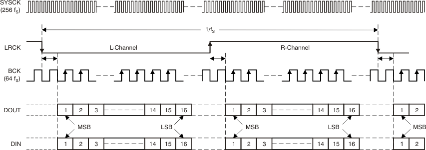 Figure 1. Audio Data Interface Format
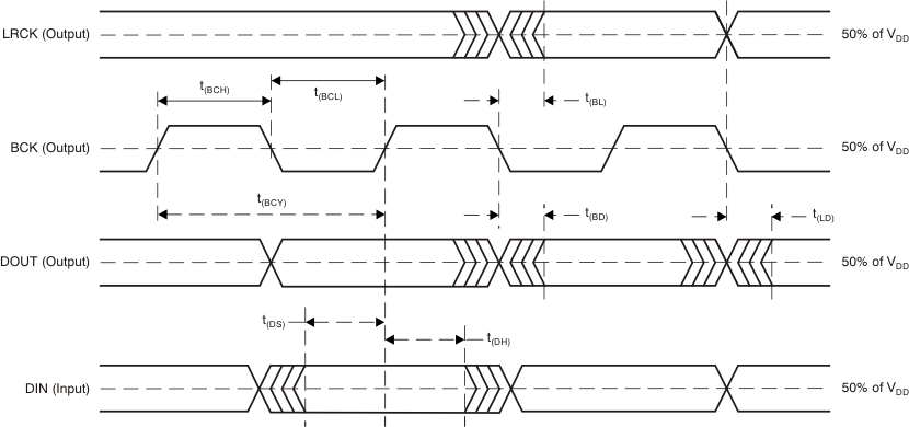 Figure 2. Audio Interface Timing
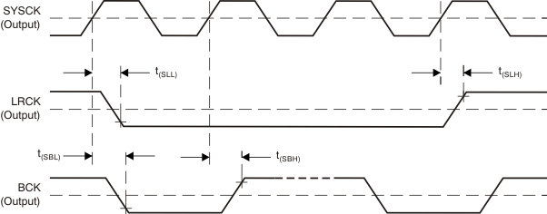 Figure 3. Audio Clock Timing
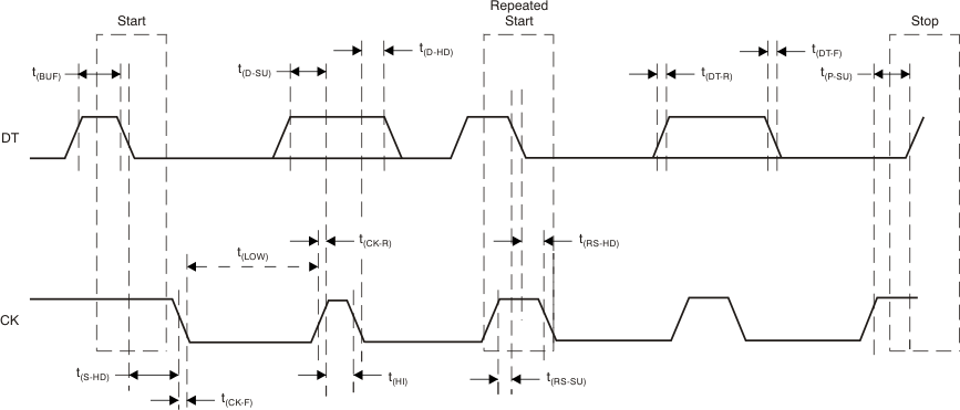 Figure 4. External ROM Read Interface Timing Requirements
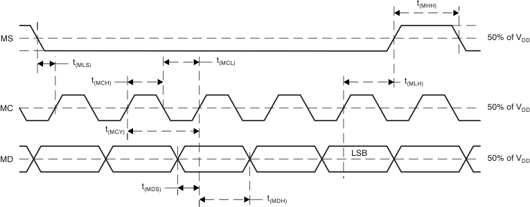 Figure 5. SPI Timing Diagram
7.11 Typical Characteristics
7.11.1 Internal Filter: DAC Digital Interpolation Filter Frequency Response
All specifications at TA = 25°C, VBUS = 5 V, ƒS = 44.1 kHz, ƒIN = 1 kHz, 16-bit data (unless otherwise noted).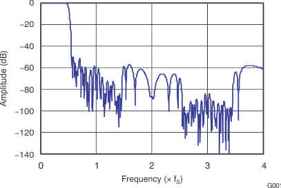 Figure 6. Frequency Response
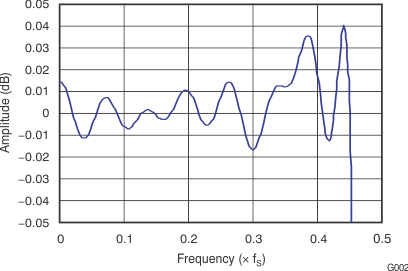 Figure 7. Passband Ripple
7.11.2 Internal Filter: DAC Analog Low-Pass Filter Frequency Response
All specifications at TA = 25°C, VBUS = 5 V, ƒS = 44.1 kHz, ƒIN = 1 kHz, 16-bit data (unless otherwise noted).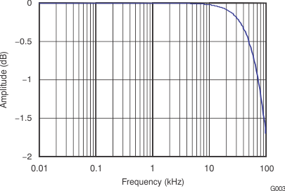 Figure 8. Passband Characteristics
 Figure 9. Stop Band Characteristics
7.11.3 General Characteristics
All specifications at TA = 25°C, VBUS = 5 V, ƒS = 44.1 kHz, ƒIN = 1 kHz, 16-bit data (unless otherwise noted). Figure 10. Total Harmonic Distortion + Noise vs Free-Air Temperature
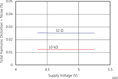 Figure 12. Total Harmonic Distortion + Noise vs Supply Voltage
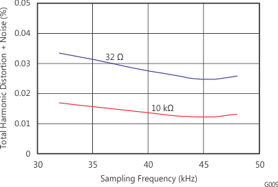 Figure 14. Total Harmonic Distortion + Noise vs Sampling Frequency
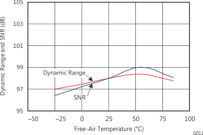 Figure 16. Dynamic Range and SNR vs Free-Air Temperature
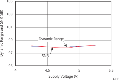 Figure 18. Dynamic Range and SNR vs Supply Voltage
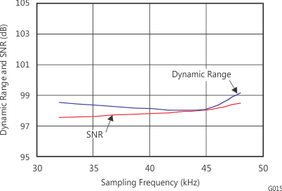 Figure 20. Dynamic Range and SNR vs Sampling Frequency
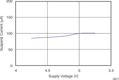 Figure 22. Suspend Current vs Supply Voltage
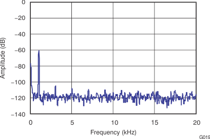 Figure 24. Output Spectrum (–60 dB, N = 8192)
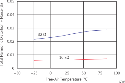 Figure 11. Total Harmonic Distortion + Noise vs Free-Air Temperature
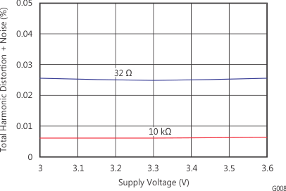 Figure 13. Total Harmonic Distortion + Noise vs Supply Voltage
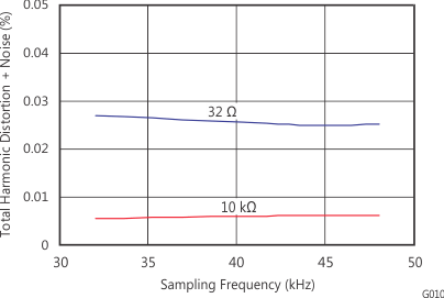 Figure 15. Total Harmonic Distortion + Noise vs Sampling Frequency
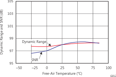 Figure 17. Dynamic Range and SNR vs Free-Air Temperature
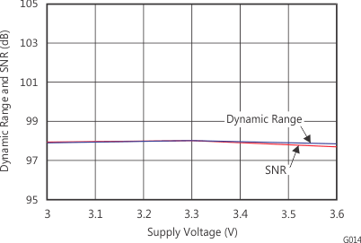 Figure 19. Dynamic Range and SNR vs Supply Voltage
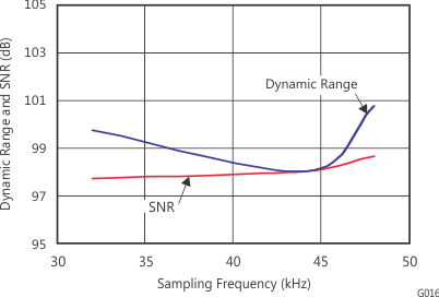 Figure 21. Dynamic Range and SNR vs Sampling Frequency
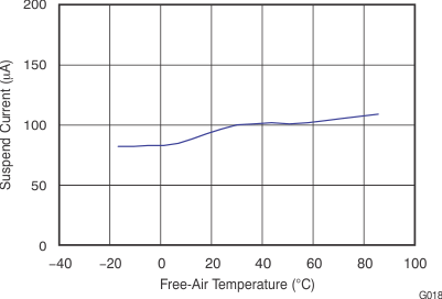 Figure 23. Suspend Current vs Free-Air Temperature
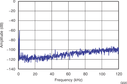 Figure 25. Output Spectrum (–60 dB, N = 8192)