ZHCSA60C May   2012  – May 2015 PCM5100A , PCM5100A-Q1 , PCM5101A , PCM5101A-Q1 , PCM5102A , PCM5102A-Q1

PRODUCTION DATA.  

  1. 特性
  2. 应用
  3. 说明
  4. 简化系统图
  5. 修订历史记录
  6. Device Comparison
  7. Pin Configuration and Functions
  8. Specifications
    1. 8.1 Absolute Maximum Ratings
    2. 8.2 ESD Ratings Updated ESD Data
    3. 8.3 Recommended Operating Conditions
    4. 8.4 Thermal Information
    5. 8.5 Electrical Characteristics
    6. 8.6 Timing Requirements
    7. 8.7 Timing Requirements, XSMT
    8. 8.8 Typical Characteristics
  9. Detailed Description
    1. 9.1 Overview
    2. 9.2 Functional Block Diagram
    3. 9.3 Feature Description
      1. 9.3.1 Terminology
      2. 9.3.2 Audio Data Interface
        1. 9.3.2.1 Audio Serial Interface
        2. 9.3.2.2 PCM Audio Data Formats
        3. 9.3.2.3 Zero Data Detect
      3. 9.3.3 XSMT Pin (Soft Mute / Soft Un-Mute)
      4. 9.3.4 Audio Processing
        1. 9.3.4.1 Interpolation Filter
      5. 9.3.5 Reset and System Clock Functions
        1. 9.3.5.1 Clocking Overview
        2. 9.3.5.2 Clock Slave Mode With Master/System Clock (SCK) Input (4 Wire I2S)
        3. 9.3.5.3 Clock Slave Mode with BCK PLL to Generate Internal Clocks (3-Wire PCM)
    4. 9.4 Device Functional Modes
      1. 9.4.1 External SCK and PLL Activation
        1. 9.4.1.1 Interpolation Filter Modes
        2. 9.4.1.2 44.1kHz De-emphasis
        3. 9.4.1.3 Audio Format
  10. 10Applications and Implementation
    1. 10.1 Application Information
      1. 10.1.1 Typical Applications
        1. 10.1.1.1 Example Design Requirements
        2. 10.1.1.2 Detailed Design Procedure
        3. 10.1.1.3 Application Curve
  11. 11Power Supply Recommendations
    1. 11.1 Power Supply Distribution and Requirements
    2. 11.2 Recommended Powerdown Sequence
      1. 11.2.1 Planned Shutdown
      2. 11.2.2 Unplanned Shutdown
    3. 11.3 External Power Sense Undervoltage Protection Mode
    4. 11.4 Power-On Reset Function
    5. 11.5 PCM510xA Power Modes
      1. 11.5.1 Setting Digital Power Supplies and I/O Voltage Rails
      2. 11.5.2 Power Save Modes
  12. 12Layout
    1. 12.1 Layout Guidelines
  13. 13器件和文档支持
    1. 13.1 相关链接
    2. 13.2 社区资源
    3. 13.3 商标
    4. 13.4 静电放电警告
  14. 14机械、封装和可订购信息
    1. 14.1 机械数据

封装选项

机械数据 (封装 | 引脚)
散热焊盘机械数据 (封装 | 引脚)
订购信息

7 Pin Configuration and Functions

PW 20-Pin Package
(Top View)
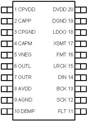
PCM5100A PCM5101A PCM5102A PCM5100A-Q1 PCM5101A-Q1 PCM5102A-Q1 po_pcm510x.gif

Pin Functions

PIN TYPE DESCRIPTION
NAME NO.
AGND 9 Analog ground
AVDD 8 P Analog power supply, 3.3 V
BCK 13 I Audio data bit clock input(1)
CAPM 4 O Charge pump flying capacitor terminal for negative rail
CAPP 2 O Charge pump flying capacitor terminal for positive rail
CPGND 3 Charge pump ground
CPVDD 1 P Charge pump power supply, 3.3 V
DEMP 10 I De-emphasis control for 44.1-kHz sampling rate(1): Off (Low) / On (High)
DGND 19 Digital ground
DIN 14 I Audio data input(1)
DVDD 20 P Digital power supply, 1.8 V or 3.3 V
FLT 11 I Filter select : Normal latency (Low) / Low latency (High)
FMT 16 I Audio format selection : I2S (Low) / Left-justified (High)
LDOO 18 P Internal logic supply rail terminal for decoupling, or external 1.8 V supply terminal
LRCK 15 I Audio data word clock input(1)
OUTL 6 O Analog output from DAC left channel
OUTR 7 O Analog output from DAC right channel
SCK 12 I System clock input(1)
VNEG 5 O Negative charge pump rail terminal for decoupling, –3.3 V
XSMT 17 I Soft mute control(1): Soft mute (Low) / soft un-mute (High)
(1) Failsafe LVCMOS Schmitt trigger input