ZHCSAC2C August   2012  – October 2018 PCM5121 , PCM5122

PRODUCTION DATA.  

  1. 特性
  2. 应用
  3. 说明
    1.     Device Images
      1.      简化系统图
  4. 修订历史记录
  5. Device Comparison
  6. Pin Configuration and Functions
    1. 6.0.1 RHB Package I2C Mode (MODE1 tied to DGND and MODE2 tied to DVDD) Top View
    2. 6.0.2 RHB Package SPI Mode (MODE1 tied to DVDD) Top View
    3. 6.0.3 RHB Package Hardwired Mode (MODE1 tied to DGND, MODE2 tied to DGND) Top View
    4.     Pin Functions
  7. Specifications
    1. 7.1 Absolute Maximum Ratings
    2. 7.2 ESD Ratings
    3. 7.3 Recommended Operating Conditions
    4. 7.4 Thermal Information
    5. 7.5 Electrical Characteristics
    6. 7.6 Timing Requirements: SCK Input
    7. 7.7 Timing Requirements: XSMT
    8. 7.8 Switching Characteristics
    9. 7.9 Typical Characteristics
  8. Detailed Description
    1. 8.1 Overview
    2. 8.2 Functional Block Diagram
    3. 8.3 Feature Description
      1. 8.3.1 Terminology
      2. 8.3.2 Audio Data Interface
        1. 8.3.2.1 Audio Serial Interface
        2. 8.3.2.2 PCM Audio Data Formats
        3. 8.3.2.3 Zero Data Detect
      3. 8.3.3 XSMT Pin (Soft Mute / Soft Un-Mute)
      4. 8.3.4 Audio Processing
        1. 8.3.4.1 PCM512x Audio Processing
          1. 8.3.4.1.1 Overview
          2. 8.3.4.1.2 Software
        2. 8.3.4.2 Interpolation Filter
        3. 8.3.4.3 Fixed Audio Processing Flow (Program 5)
          1. 8.3.4.3.1 Filter Programming Changes
          2. 8.3.4.3.2 Processing Blocks – Detailed Descriptions
          3. 8.3.4.3.3 Biquad Section
          4. 8.3.4.3.4 Dynamic Range Compression
          5. 8.3.4.3.5 Stereo Mixer
          6. 8.3.4.3.6 Stereo Multiplexer
          7. 8.3.4.3.7 Mono Mixer
          8. 8.3.4.3.8 Master Volume Control
          9. 8.3.4.3.9 Miscellaneous Coefficients
      5. 8.3.5 DAC Outputs
        1. 8.3.5.1 Analog Outputs
        2. 8.3.5.2 Recommended Output Filter for the PCM512x
        3. 8.3.5.3 Choosing Between VREF and VCOM Modes
          1. 8.3.5.3.1 Voltage Reference and Output Levels
          2. 8.3.5.3.2 Mode Switching Sequence, from VREF Mode to VCOM Mode
        4. 8.3.5.4 Digital Volume Control
          1. 8.3.5.4.1 Emergency Ramp-Down
        5. 8.3.5.5 Analog Gain Control
      6. 8.3.6 Reset and System Clock Functions
        1. 8.3.6.1 Clocking Overview
        2. 8.3.6.2 Clock Slave Mode With Master and System Clock (SCK) Input (4 Wire I2S)
        3. 8.3.6.3 Clock Slave Mode With BCK PLL to Generate Internal Clocks (3-Wire PCM)
        4. 8.3.6.4 Clock Generation Using the PLL
        5. 8.3.6.5 PLL Calculation
          1. 8.3.6.5.1 Examples:
            1. 8.3.6.5.1.1 Recommended PLL Settings
        6. 8.3.6.6 Clock Master Mode from Audio Rate Master Clock
        7. 8.3.6.7 Clock Master from a Non-Audio Rate Master Clock
    4. 8.4 Device Functional Modes
      1. 8.4.1 Choosing a Control Mode
        1. 8.4.1.1 Software Control
          1. 8.4.1.1.1 SPI Interface
            1. 8.4.1.1.1.1 Register Read and Write Operation
          2. 8.4.1.1.2 I2C Interface
            1. 8.4.1.1.2.1 Slave Address
            2. 8.4.1.1.2.2 Register Address Auto-Increment Mode
            3. 8.4.1.1.2.3 Packet Protocol
            4. 8.4.1.1.2.4 Write Register
            5. 8.4.1.1.2.5 Read Register
            6. 8.4.1.1.2.6 Timing Characteristics
      2. 8.4.2 VREF and VCOM Modes
    5. 8.5 Programming
  9. Application and Implementation
    1. 9.1 Application Information
    2. 9.2 Typical Application
      1. 9.2.1 Design Requirements
      2. 9.2.2 Detailed Design Procedure
      3. 9.2.3 Application Curve
  10. 10Power Supply Recommendations
    1. 10.1 Power Supply Distribution and Requirements
    2. 10.2 Recommended Powerdown Sequence
      1. 10.2.1 XSMT = 0
      2. 10.2.2 Clock Error Detect
      3. 10.2.3 Planned Shutdown
      4. 10.2.4 Unplanned Shutdown
    3. 10.3 External Power Sense Undervoltage Protection Mode
    4. 10.4 Power-On Reset Function
      1. 10.4.1 Power-On Reset, DVDD 3.3-V Supply
      2. 10.4.2 Power-On Reset, DVDD 1.8-V Supply
    5. 10.5 PCM512x Power Modes
      1. 10.5.1 Setting Digital Power Supplies and I/O Voltage Rails
      2. 10.5.2 Power Save Modes
      3. 10.5.3 Power Save Parameter Programming
  11. 11Layout
    1. 11.1 Layout Guidelines
    2. 11.2 Layout Example
  12. 12Register Maps
    1. 12.1 PCM512x Register Map
      1. 12.1.1 Detailed Register Descriptions
        1. 12.1.1.1 Register Map Summary
        2. 12.1.1.2 Page 0 Registers
        3. 12.1.1.3 Page 1 Registers
        4. 12.1.1.4 Page 44 Registers
        5. 12.1.1.5 Page 253 Registers
      2. 12.1.2 PLL Tables for Software Controlled Devices
      3. 12.1.3 Coefficient Data Formats
      4. 12.1.4 Power Down and Reset Behavior
  13. 13器件和文档支持
    1. 13.1 开发支持
    2. 13.2 文档支持
    3. 13.3 相关链接
    4. 13.4 接收文档更新通知
    5. 13.5 社区资源
    6. 13.6 商标
    7. 13.7 静电放电警告
    8. 13.8 术语表
  14. 14机械、封装和可订购信息

封装选项

机械数据 (封装 | 引脚)
散热焊盘机械数据 (封装 | 引脚)
订购信息

PCM Audio Data Formats

The PCM512x supports industry-standard audio data formats, including standard I2S and left-justified. Data formats are selected via Register (Pg0Reg40). All formats require binary twos-complement, MSB-first audio data; up to 32-bit audio data is accepted.

The PCM512x also supports right-justified and TDM/DSP in software control mode. I2S, LJ, RJ, and TDM/DSP are selected using Register (Pg0Reg40). All formats require binary twos-complement, MSB-first audio data. Up to 32 bits are accepted. Default setting is I2S and 24-bit word length.
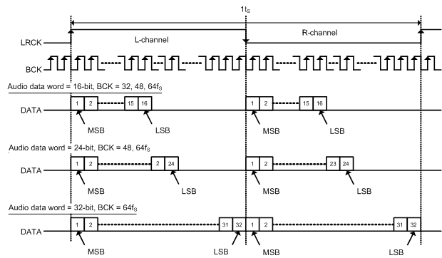
PCM5121 PCM5122 f_pcm51xx_aud_data_format_lj.gifFigure 13. Left-Justified Audio Data Format
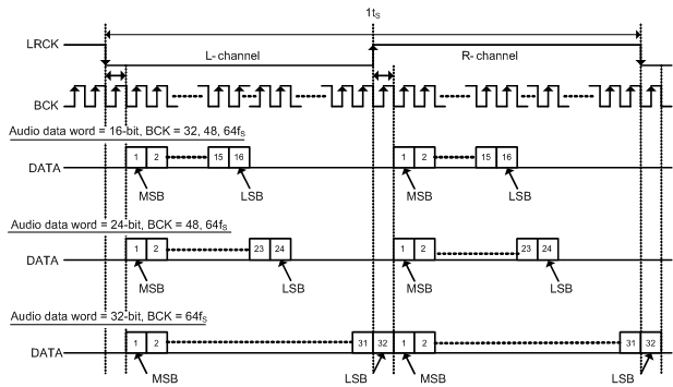
PCM5121 PCM5122 f_pcm51xx_aud_data_format_i2s.gif
I2S Data Format; L-channel = LOW, R-channel = HIGH
Figure 14. I2S Audio Data Format

The following data formats are only available in software mode.
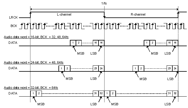
PCM5121 PCM5122 f_pcm51xx_aud_data_format_rj.gif
Right Justified Data Format; L-channel = HIGH, R-channel = LOW
Figure 15. Right-Justified Audio Data Format
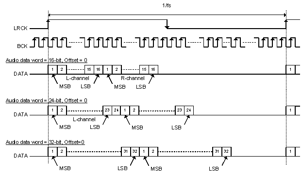
PCM5121 PCM5122 f_pcm51xx_aud_data_format_tdm1.gif
TDM/DSP Data Format; L-channel = FIRST, R-channel = LAST with OFFSET = 0
Figure 16. TDM/DSP 1 Audio Data Format

NOTE

In TDM Modes, Duty Cycle of LRCK should be 1x BCK at minimum. Rising edge is considered frame start.
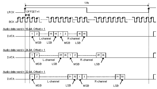
PCM5121 PCM5122 f_pcm51xx_aud_data_format_tdm2.gif
TDM/DSP Data Format; L-channel = FIRST, R-channel = LAST with OFFSET = 1
Figure 17. TDM/DSP 2 Audio Data Format
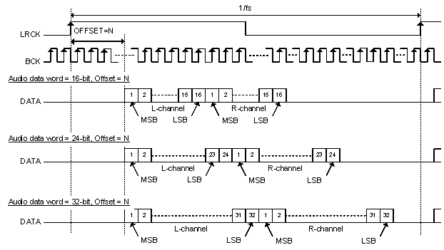
PCM5121 PCM5122 f_pcm51xx_aud_data_format_tdm3.gif
TDM/DSP Data Format; L-channel = FIRST, R-channel = LAST with OFFSET = N
Figure 18. TDM/DSP 3 Audio Data Format