ZHCSAC2C August 2012 – October 2018 PCM5121 , PCM5122
PRODUCTION DATA.
- 1 特性
- 2 应用
- 3 说明
- 4 修订历史记录
- 5 Device Comparison
- 6 Pin Configuration and Functions
- 7 Specifications
-
8 Detailed Description
- 8.1 Overview
- 8.2 Functional Block Diagram
- 8.3
Feature Description
- 8.3.1 Terminology
- 8.3.2 Audio Data Interface
- 8.3.3 XSMT Pin (Soft Mute / Soft Un-Mute)
- 8.3.4 Audio Processing
- 8.3.5 DAC Outputs
- 8.3.6
Reset and System Clock Functions
- 8.3.6.1 Clocking Overview
- 8.3.6.2 Clock Slave Mode With Master and System Clock (SCK) Input (4 Wire I2S)
- 8.3.6.3 Clock Slave Mode With BCK PLL to Generate Internal Clocks (3-Wire PCM)
- 8.3.6.4 Clock Generation Using the PLL
- 8.3.6.5 PLL Calculation
- 8.3.6.6 Clock Master Mode from Audio Rate Master Clock
- 8.3.6.7 Clock Master from a Non-Audio Rate Master Clock
- 8.4 Device Functional Modes
- 8.5 Programming
- 9 Application and Implementation
- 10Power Supply Recommendations
- 11Layout
- 12Register Maps
- 13器件和文档支持
- 14机械、封装和可订购信息
8.3.6.1 Clocking Overview
The PCM512x devices have flexible systems for clocking. Internally, the device requires a number of clocks, mostly at related clock rates to function correctly. All of these clocks can be derived from the serial audio interface in one form or another.
 Figure 62. Audio Flow with Respective Clocks
 As shown in Figure 62 the data flows at the sample rate (fS). Once the data is brought into the serial audio interface, it gets processed, interpolated and modulated all the way to 128 × fS before arriving at the current segments for the final digital to analog conversion.
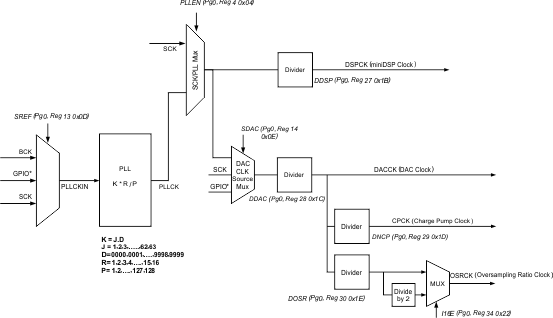
The clock tree is shown in Figure 63.
 Figure 63. PCM512x Clock Distribution Tree
 The serial audio interface typically has 4 connections: SCK (system master clock), BCK (bit clock), LRCK (left right word clock), and DIN (data). The device has an internal PLL that is used to take either SCK or BCK and create the higher rate clocks required by the interpolating processor and the DAC clock. This allows the device to operate with or without an external SCK.
In situations where the highest audio performance is required, it is suggested that the SCK is brought to the device, along with BCK and LRCK. The device should be configured so that the PLL is only providing a clock source to the audio processing block. By ensuring that the DACCK (DAC Clock) is being driven by the external SCK source, jitter evident in the PLL (in all PLLs) is kept out of the DAC, charge pump, and oversampling system.
Everything else should be a division of the incoming SCK. This is done by setting DAC CLK Source Mux (SDAC in Figure 63) to use SCK as a source, rather than the output of the SCK/PLL Mux. Code examples for this are available in SLASE12.
When the Auto Clock Configuration bit is set (Page 0/ Register 0x25), no additional clocks configuration is required. However, when setting custom PLL values and so forth, the target output rates should match those shown in the recommended PLL values of Table 131.