ZHCSAC2C August   2012  – October 2018 PCM5121 , PCM5122

PRODUCTION DATA.  

  1. 特性
  2. 应用
  3. 说明
    1.     Device Images
      1.      简化系统图
  4. 修订历史记录
  5. Device Comparison
  6. Pin Configuration and Functions
    1. 6.0.1 RHB Package I2C Mode (MODE1 tied to DGND and MODE2 tied to DVDD) Top View
    2. 6.0.2 RHB Package SPI Mode (MODE1 tied to DVDD) Top View
    3. 6.0.3 RHB Package Hardwired Mode (MODE1 tied to DGND, MODE2 tied to DGND) Top View
    4.     Pin Functions
  7. Specifications
    1. 7.1 Absolute Maximum Ratings
    2. 7.2 ESD Ratings
    3. 7.3 Recommended Operating Conditions
    4. 7.4 Thermal Information
    5. 7.5 Electrical Characteristics
    6. 7.6 Timing Requirements: SCK Input
    7. 7.7 Timing Requirements: XSMT
    8. 7.8 Switching Characteristics
    9. 7.9 Typical Characteristics
  8. Detailed Description
    1. 8.1 Overview
    2. 8.2 Functional Block Diagram
    3. 8.3 Feature Description
      1. 8.3.1 Terminology
      2. 8.3.2 Audio Data Interface
        1. 8.3.2.1 Audio Serial Interface
        2. 8.3.2.2 PCM Audio Data Formats
        3. 8.3.2.3 Zero Data Detect
      3. 8.3.3 XSMT Pin (Soft Mute / Soft Un-Mute)
      4. 8.3.4 Audio Processing
        1. 8.3.4.1 PCM512x Audio Processing
          1. 8.3.4.1.1 Overview
          2. 8.3.4.1.2 Software
        2. 8.3.4.2 Interpolation Filter
        3. 8.3.4.3 Fixed Audio Processing Flow (Program 5)
          1. 8.3.4.3.1 Filter Programming Changes
          2. 8.3.4.3.2 Processing Blocks – Detailed Descriptions
          3. 8.3.4.3.3 Biquad Section
          4. 8.3.4.3.4 Dynamic Range Compression
          5. 8.3.4.3.5 Stereo Mixer
          6. 8.3.4.3.6 Stereo Multiplexer
          7. 8.3.4.3.7 Mono Mixer
          8. 8.3.4.3.8 Master Volume Control
          9. 8.3.4.3.9 Miscellaneous Coefficients
      5. 8.3.5 DAC Outputs
        1. 8.3.5.1 Analog Outputs
        2. 8.3.5.2 Recommended Output Filter for the PCM512x
        3. 8.3.5.3 Choosing Between VREF and VCOM Modes
          1. 8.3.5.3.1 Voltage Reference and Output Levels
          2. 8.3.5.3.2 Mode Switching Sequence, from VREF Mode to VCOM Mode
        4. 8.3.5.4 Digital Volume Control
          1. 8.3.5.4.1 Emergency Ramp-Down
        5. 8.3.5.5 Analog Gain Control
      6. 8.3.6 Reset and System Clock Functions
        1. 8.3.6.1 Clocking Overview
        2. 8.3.6.2 Clock Slave Mode With Master and System Clock (SCK) Input (4 Wire I2S)
        3. 8.3.6.3 Clock Slave Mode With BCK PLL to Generate Internal Clocks (3-Wire PCM)
        4. 8.3.6.4 Clock Generation Using the PLL
        5. 8.3.6.5 PLL Calculation
          1. 8.3.6.5.1 Examples:
            1. 8.3.6.5.1.1 Recommended PLL Settings
        6. 8.3.6.6 Clock Master Mode from Audio Rate Master Clock
        7. 8.3.6.7 Clock Master from a Non-Audio Rate Master Clock
    4. 8.4 Device Functional Modes
      1. 8.4.1 Choosing a Control Mode
        1. 8.4.1.1 Software Control
          1. 8.4.1.1.1 SPI Interface
            1. 8.4.1.1.1.1 Register Read and Write Operation
          2. 8.4.1.1.2 I2C Interface
            1. 8.4.1.1.2.1 Slave Address
            2. 8.4.1.1.2.2 Register Address Auto-Increment Mode
            3. 8.4.1.1.2.3 Packet Protocol
            4. 8.4.1.1.2.4 Write Register
            5. 8.4.1.1.2.5 Read Register
            6. 8.4.1.1.2.6 Timing Characteristics
      2. 8.4.2 VREF and VCOM Modes
    5. 8.5 Programming
  9. Application and Implementation
    1. 9.1 Application Information
    2. 9.2 Typical Application
      1. 9.2.1 Design Requirements
      2. 9.2.2 Detailed Design Procedure
      3. 9.2.3 Application Curve
  10. 10Power Supply Recommendations
    1. 10.1 Power Supply Distribution and Requirements
    2. 10.2 Recommended Powerdown Sequence
      1. 10.2.1 XSMT = 0
      2. 10.2.2 Clock Error Detect
      3. 10.2.3 Planned Shutdown
      4. 10.2.4 Unplanned Shutdown
    3. 10.3 External Power Sense Undervoltage Protection Mode
    4. 10.4 Power-On Reset Function
      1. 10.4.1 Power-On Reset, DVDD 3.3-V Supply
      2. 10.4.2 Power-On Reset, DVDD 1.8-V Supply
    5. 10.5 PCM512x Power Modes
      1. 10.5.1 Setting Digital Power Supplies and I/O Voltage Rails
      2. 10.5.2 Power Save Modes
      3. 10.5.3 Power Save Parameter Programming
  11. 11Layout
    1. 11.1 Layout Guidelines
    2. 11.2 Layout Example
  12. 12Register Maps
    1. 12.1 PCM512x Register Map
      1. 12.1.1 Detailed Register Descriptions
        1. 12.1.1.1 Register Map Summary
        2. 12.1.1.2 Page 0 Registers
        3. 12.1.1.3 Page 1 Registers
        4. 12.1.1.4 Page 44 Registers
        5. 12.1.1.5 Page 253 Registers
      2. 12.1.2 PLL Tables for Software Controlled Devices
      3. 12.1.3 Coefficient Data Formats
      4. 12.1.4 Power Down and Reset Behavior
  13. 13器件和文档支持
    1. 13.1 开发支持
    2. 13.2 文档支持
    3. 13.3 相关链接
    4. 13.4 接收文档更新通知
    5. 13.5 社区资源
    6. 13.6 商标
    7. 13.7 静电放电警告
    8. 13.8 术语表
  14. 14机械、封装和可订购信息

封装选项

机械数据 (封装 | 引脚)
散热焊盘机械数据 (封装 | 引脚)
订购信息

External Power Sense Undervoltage Protection Mode

NOTE

External Power Sense Undervoltage Protection Mode is supported only when
DVDD = 3.3 V.

The XSMT pin can also be used to monitor a system voltage, such as the 24-VDC LCD TV backlight, or 12-VDC system supply using a voltage divider created with two resistors. (See Figure 81.)

  • If the XSMT pin makes a transition from 1 to 0 over 6 ms or more, the device switches into external undervoltage protection mode. This mode uses two trigger levels:
    • When the XSMT pin level reaches 2 V, soft mute process begins.
    • When the XSMT pin level reaches 1.2 V, analog mute engages, regardless of digital audio level, and analog shutdown begins. (DAC and related circuitry powers down).

If XSMT is moved from 1 to 0 in 20 ns or less, then the device will interpret it as a digital controlled request to mute. It will perform a soft mute, then move to standby.

A timing diagram to show this is shown in Figure 82.

NOTE

The XSMT input pin voltage range is from –0.3 V to DVDD + 0.3 V. The ratio of external resistors must produce a voltage within this input range. Any increase in power supply (such as power supply positive noise or ripple) can pull the XSMT pin higher than DVDD + 0.3 V.

For example, if the PCM512x is monitoring a 12-V input, and dividing the voltage by 4, then the voltage at XSMT during ideal power supply conditions is 3.3 V. A voltage spike higher than 14.4 V causes a voltage greater than 3.6 V (DVDD + 0.3) on the XSMT pin, potentially damaging the device.

Providing the divider is set appropriately, any DC voltage can be monitored.
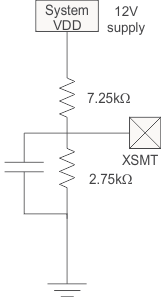
PCM5121 PCM5122 f_pcm51xx_xsmt_ext_uvp_ckt.gifFigure 81. XSMT in External UVP Mode
PCM5121 PCM5122 f_pcm51xx_td_xsmt_uvp.gifFigure 82. XSMT Timing for Undervoltage Protection

The trigger voltage values for the soft mute and hard mute are shown in Table 47. The range of values will vary from device to device, but typical thresholds are shown. XSMT should be set up to nominally be 3.3 V along with DVDD, but derived from a higher system power supply rail.

Table 47. Distribution of Voltage Thresholds

MIN TYP MAX UNIT
Soft Mute Threshold Voltage 2 2.2 0.9 × DVDD V
Hard Mute Threshold Voltage 0.1 × DVDD 0.9 1.2 V