SBOS424C March 2008 – November 2015 PGA112 , PGA113 , PGA116 , PGA117
PRODUCTION DATA.
- 1 Features
- 2 Applications
- 3 Description
- 4 Revision History
- 5 Device Comparison
- 6 Pin Configuration and Functions
- 7 Specifications
- 8 Detailed Description
-
9 Applications and Implementation
- 9.1
Application Information
- 9.1.1 Op Amp: Input Stage
- 9.1.2 Op Amp: General Gain Equations
- 9.1.3 Op Amp: Frequency Response Versus Gain
- 9.1.4 Analog MUX
- 9.1.5 System Calibration Using The PGA
- 9.1.6 Driving and Interfacing to ADCs
- 9.1.7 Power Supplies
- 9.1.8 Shutdown and Power-On-Reset (POR)
- 9.1.9 Typical Connections: PGA116, PGA117 (TSSOP-20)
- 9.2 Typical Applications
- 9.1
Application Information
- 10Power Supply Recommendations
- 11Layout
- 12Device and Documentation Support
- 13Mechanical, Packaging, and Orderable Information
11 Layout
11.1 Layout Guidelines
11.1.1 High Gain and Wide Bandwidth Considerations
As a result of the combination of wide bandwidth and high gain capability of the PGA112 and PGA113 devices and PGA116 and PGA117 devices, there are several printed-circuit-board (PCB) design and system recommendations to consider for optimum application performance.
- Power-supply bypass: Refer to Power Supply Recommendations.
- Signal trace routing: Keep VOUT and other low impedance traces away from MUX channel inputs that are high impedance. Poor signal routing can cause positive feedback, unwanted oscillations, or excessive overshoot and ringing on step-changing signals. If the input signals are particularly noisy, separate MUX input channels with guard traces on either side of the signal traces. Connect the guard traces to ground near the PGA and at the signal entry point into the PCB. On multilayer PCBs, ensure that there are no parallel traces near MUX input traces on adjacent layers; capacitive coupling from other layers can be a problem. Use ground planes to isolate MUX input signal traces from signal traces on other layers.
-
Input MUX channels and source impedance: Input MUX channels are high-impedance; when combined with high gain, the channels can pick up unwanted noise. Keep the input signal sources low-impedance
(< 10 kΩ). Also, consider bypassing input MUX channels with a ceramic bypass capacitor directly at the MUX input pin. Bypass capacitors greater than 100 pF are recommended. Lower impedances and a bypass capacitor placed directly at the input MUX channels keep crosstalk between channels to a minimum as a result of parasitic capacitive coupling from adjacent PCB traces and pin-to-pin capacitance.
Additionally, group and route the digital signals into the PGA as far away as possible from the analog MUX input signals. Most digital signals are fast rise and fall time signals with low-impedance drive capability that can easily couple into the high-impedance inputs of the input MUX channels. This coupling can create unwanted noise that gains up to VOUT.
11.2 Layout Example
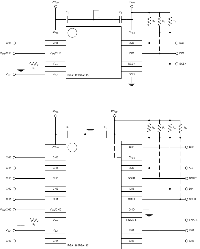
 Figure 82. PGA11x Layout Example