SBOS424C March 2008 – November 2015 PGA112 , PGA113 , PGA116 , PGA117
PRODUCTION DATA.
- 1 Features
- 2 Applications
- 3 Description
- 4 Revision History
- 5 Device Comparison
- 6 Pin Configuration and Functions
- 7 Specifications
- 8 Detailed Description
-
9 Applications and Implementation
- 9.1
Application Information
- 9.1.1 Op Amp: Input Stage
- 9.1.2 Op Amp: General Gain Equations
- 9.1.3 Op Amp: Frequency Response Versus Gain
- 9.1.4 Analog MUX
- 9.1.5 System Calibration Using The PGA
- 9.1.6 Driving and Interfacing to ADCs
- 9.1.7 Power Supplies
- 9.1.8 Shutdown and Power-On-Reset (POR)
- 9.1.9 Typical Connections: PGA116, PGA117 (TSSOP-20)
- 9.2 Typical Applications
- 9.1
Application Information
- 10Power Supply Recommendations
- 11Layout
- 12Device and Documentation Support
- 13Mechanical, Packaging, and Orderable Information
6 Pin Configuration and Functions
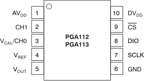
DGS Package
10-Pin VSSOP
Top View

Pin Functions: PGA112, PGA113
| PIN | I/O | DESCRIPTION | |
|---|---|---|---|
| NO. | NAME | ||
| 1 | AVDD | I | Analog supply voltage (2.2 V to 5.5 V) |
| 2 | CH1 | I | Input MUX channel 1 |
| 3 | VCAL/CH0 | I | Input MUX channel 0 and VCAL input. For system calibration purposes, connect this pin to a low-impedance external reference voltage to use internal calibration channels. The four internal calibration channels are connected to GND, 0.9 VCAL, 0.1 VCAL, and VREF, respectively. VCAL is loaded with 100 kΩ (typical) when internal calibration channels CAL2 or CAL3 are selected. Otherwise, VCAL/CH0 appears as high impedance. |
| 4 | VREF | I | Reference input pin. Connect external reference for VOUT offset shift or to midsupply for midsupply referenced systems. VREF must be connected to a low-impedance reference capable of sourcing and sinking at least 2 mA or VREF must be connected to GND. |
| 5 | VOUT | O | Analog voltage output. When AVDD < DVDD, VOUT is clamped to AVDD + 300 mV. |
| 6 | GND | — | Ground pin |
| 7 | SCLK | I | Clock input for SPI serial interface |
| 8 | DIO | I | Data input/output for SPI serial interface. DIO contains a weak, 10-μA internal pulldown current source. |
| 9 | CS | I | Chip select line for SPI serial interface |
| 10 | DVDD | I | Digital and op amp output stage supply voltage (2.2 V to 5.5 V). Useful in multi-supply systems to prevent overvoltage and lockup condition on an analog-to-digital (ADC) input (for example, a microcontroller with an ADC running on 3 V and the PGA powered from 5 V). Digital I/O levels to be relative to DVDD. DVDD should be bypassed with a 0.1-μF ceramic capacitor, and DVDD must supply the current for the digital portion of the PGA as well as the load current for the op amp output stage. |
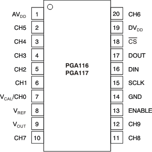
PW Package
20-Pin TSSOP
Top View

Pin Functions: PGA116, PGA117
| PIN | I/O | DESCRIPTION | |
|---|---|---|---|
| NO. | NAME | ||
| 1 | AVDD | I | Analog supply voltage (2.2 V to 5.5 V) |
| 2 | CH5 | I | Input MUX channel 5 |
| 3 | CH4 | I | Input MUX channel 4 |
| 4 | CH3 | I | Input MUX channel 3 |
| 5 | CH2 | I | Input MUX channel 2 |
| 6 | CH1 | I | Input MUX channel 1 |
| 7 | VCAL/CH0 | I | Input MUX channel 0 and VCAL input. For system calibration purposes, connect this pin to a low-impedance external reference voltage to use internal calibration channels. The four internal calibration channels are connected to GND, 0.9 VCAL, 0.1 VCAL, and VREF, respectively. VCAL is loaded with 100 kΩ (typical) when internal calibration channels CAL2 or CAL3 are selected. Otherwise, VCAL/CH0 appears as high impedance. |
| 8 | VREF | I | Reference input pin. Connect external reference for VOUT offset shift or to midsupply for midsupply referenced systems. VREF must be connected to a low-impedance reference capable of sourcing and sinking at least 2 mA or to GND. |
| 9 | VOUT | O | Analog voltage output. When AVDD < DVDD, VOUT is clamped to AVDD + 300 mV. |
| 10 | CH7 | I | Input MUX channel 7 |
| 11 | CH8 | I | Input MUX channel 8 |
| 12 | CH9 | I | Input MUX channel 9 |
| 13 | ENABLE | I | Hardware enable pin. Logic low puts the part into Shutdown mode (IQ < 1 μA). |
| 14 | GND | — | Ground pin |
| 15 | SCLK | I | Clock input for SPI serial interface |
| 16 | DIN | I | Data input for SPI serial interface. DIN contains a weak, 10-μA internal pulldown current source to allow for ease of daisy-chain configurations. |
| 17 | DOUT | O | Data output for SPI serial interface. DOUT goes to high-Z state when CS goes high for standard SPI interface. |
| 18 | CS | I | Chip select line for SPI serial interface |
| 19 | DVDD | I | Digital and op amp output stage supply voltage (2.2 V to 5.5 V). Useful in multi-supply systems to prevent overvoltage and lockup condition on an ADC input (for example, a microcontroller with an ADC running on 3 V and the PGA powered from 5 V). Digital I/O levels to be relative to DVDD. DVDD should be bypassed with a 0.1-μF ceramic capacitor, and DVDD must supply the current for the digital portion of the PGA as well as the load current for the op amp output stage. |
| 20 | CH6 | I | Input MUX channel 6 |