SBOS424C March 2008 – November 2015 PGA112 , PGA113 , PGA116 , PGA117
PRODUCTION DATA.
- 1 Features
- 2 Applications
- 3 Description
- 4 Revision History
- 5 Device Comparison
- 6 Pin Configuration and Functions
- 7 Specifications
- 8 Detailed Description
-
9 Applications and Implementation
- 9.1
Application Information
- 9.1.1 Op Amp: Input Stage
- 9.1.2 Op Amp: General Gain Equations
- 9.1.3 Op Amp: Frequency Response Versus Gain
- 9.1.4 Analog MUX
- 9.1.5 System Calibration Using The PGA
- 9.1.6 Driving and Interfacing to ADCs
- 9.1.7 Power Supplies
- 9.1.8 Shutdown and Power-On-Reset (POR)
- 9.1.9 Typical Connections: PGA116, PGA117 (TSSOP-20)
- 9.2 Typical Applications
- 9.1
Application Information
- 10Power Supply Recommendations
- 11Layout
- 12Device and Documentation Support
- 13Mechanical, Packaging, and Orderable Information
7 Specifications
7.1 Absolute Maximum Ratings
Over operating free-air temperature range, unless otherwise noted.(1)| MIN | MAX | UNIT | ||
|---|---|---|---|---|
| Supply voltage | 7 | V | ||
| Signal input terminals, voltage(2) | GND – 0.5 | AVDD + 0.5 | V | |
| Signal input terminals, current(2) | ±10 | mA | ||
| Output short circuit | Continuous | |||
| Operating temperature | –40 | 125 | °C | |
| Junction temperature | 150 | °C | ||
| Storage temperature | –65 | 150 | °C | |
(1) Stresses above these ratings may cause permanent damage. Exposure to absolute maximum conditions for extended periods may degrade device reliability. These are stress ratings only, and functional operation of the device at these or any other conditions beyond those specified is not implied.
(2) Input terminals are diode-clamped to the power-supply rails. Input signals that can swing more than 0.5 V beyond the supply rails should be current-limited to 10 mA or less.
7.2 ESD Ratings
| VALUE | UNIT | |||
|---|---|---|---|---|
| V(ESD) | Electrostatic discharge | Human-body model (HBM), per ANSI/ESDA/JEDEC JS-001(1) | ±3000 | V |
| Charged-device model (CDM), per JEDEC specification JESD22-C101(2) | ±1000 | |||
| Machine Model (MM) | ±300 | |||
(1) JEDEC document JEP155 states that 500-V HBM allows safe manufacturing with a standard ESD control process.
(2) JEDEC document JEP157 states that 250-V CDM allows safe manufacturing with a standard ESD control process.
7.3 Recommended Operating Conditions
over operating free-air temperature range (unless otherwise noted)| MIN | NOM | MAX | UNIT | ||
|---|---|---|---|---|---|
| AVDD | 2.2 | 5 | 5.5 | V | |
| DVDD | 2.2 | 5 | 5.5 | V | |
| Operating temperature | –40 | 25 | 125 | °C | |
7.4 Thermal Information
| THERMAL METRIC(1) | PGA112, PGA113 | PGA116, PGA117 | UNIT | |
|---|---|---|---|---|
| DGS (VSSOP) | PW (TSSOP) | |||
| 10 PINS | 20 PINS | |||
| RθJA | Junction-to-ambient thermal resistance | 98.3 | 100.3 | °C/W |
| RθJC(top) | Junction-to-case (top) thermal resistance | 57 | 36.9 | °C/W |
| RθJB | Junction-to-board thermal resistance | 51.2 | 50.6 | °C/W |
| ψJT | Junction-to-top characterization parameter | 1.3 | 2.6 | °C/W |
| ψJB | Junction-to-board characterization parameter | 36.9 | 50.2 | °C/W |
| RθJC(bot) | Junction-to-case (bottom) thermal resistance | 4.8 | N/A | °C/W |
(1) For more information about traditional and new thermal metrics, see the IC Package Thermal Metrics application report, SPRA953.
7.5 Electrical Characteristics: VS = AVDD = DVDD = 5 V
at TA = 25°C, RL = 10kΩ//CL = 100 pF connected to DVDD/2, and VREF = GND (unless otherwise noted)| PARAMETER | TEST CONDITIONS | MIN | TYP | MAX | UNIT | |||
|---|---|---|---|---|---|---|---|---|
| OFFSET VOLTAGE | ||||||||
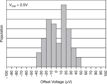
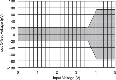
| Input offset voltage | VOS | AVDD = DVDD = 5 V, VREF = VIN = AVDD/2, VCM = 2.5 V | ±25 | ±100 | μV | |||
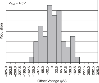
| AVDD = DVDD = 5 V, VREF = VIN = AVDD/2, VCM = 4.5 V | ±75 | ±325 | μV | |||||
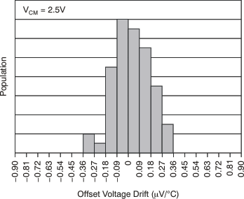
| vs temperature, –40°C to 125°C | dVOS/dT | AVDD = DVDD = 5 V, VCM = 2.5 V | TA = –40°C to 125°C | 0.35 | 1.2 | μV/°C | ||
| vs temperature, –40°C to 85°C | AVDD = DVDD = 5 V, VCM = 2.5 V | 0.15 | 0.9 | μV/°C | ||||
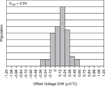
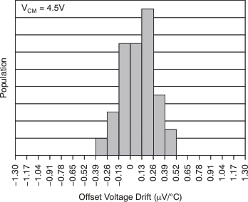
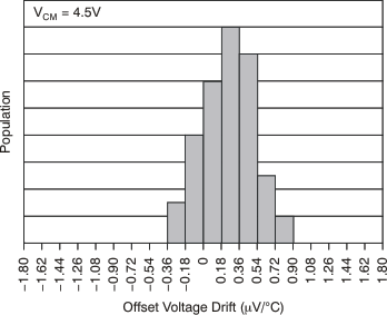
| vs temperature, –40°C to 125°C | AVDD = DVDD = 5 V, VCM = 4.5 V | TA = –40°C to 125°C | 0.6 | 1.8 | μV/°C | |||
| vs temperature, –40°C to 85°C | AVDD = DVDD = 5 V, VCM = 4.5 V | 0.3 | 1.3 | μV/°C | ||||
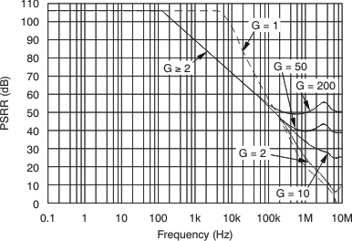
| vs power supply | PSRR | AVDD = DVDD = 2.2 V to 5.5 V, VCM = 0.5 V, VREF = VIN = AVDD/2 |
5 | 20 | μV/V | |||
| Over temperature, –40°C to 125°C | AVDD = DVDD = 2.2 V to 5.5 V, VCM = 0.5 V, VREF = VIN = AVDD/2 |
TA = –40°C to 125°C | 5 | 40 | μV/V | |||
| INPUT ON-CHANNEL CURRENT | ||||||||
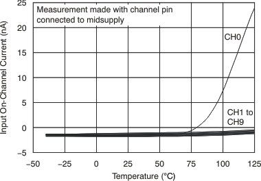
| Input on-channel current (Ch0, Ch1) | IIN | VREF = VIN = AVDD/2 | ±1.5 | ±5 | nA | |||
| Over temperature, –40°C to 125°C | VREF = VIN = AVDD/2 | See Typical Characteristics | nA | |||||
| INPUT VOLTAGE RANGE | ||||||||
| Input voltage range(1) | IVR | GND – 0.1 | AVDD + 0.1 | V | ||||
| Overvoltage input range | No output phase reversal(2) | GND – 0.3 | AVDD + 0.3 | V | ||||
| INPUT IMPEDANCE (Channel On)(3) | ||||||||
| Channel input capacitance | CCH | 2 | pF | |||||
| Channel switch resistance | RSW | 150 | Ω | |||||
| Amplifier input capacitance | CAMP | 3 | pF | |||||
| Amplifier input resistance | RAMP | Input resistance to GND | 10 | GΩ | ||||
| VCAL/CH0 | RIN | CAL1 or CAL2 selected | 100 | kΩ | ||||
| GAIN SELECTIONS | ||||||||
| Nominal gains | Binary gains: 1, 2, 4, 8, 16, 32, 64, 128 | 1 | 128 | |||||
| Scope gains: 1, 2, 5, 10, 20, 50, 100, 200 | 1 | 200 | ||||||
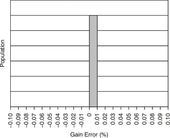
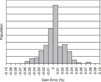
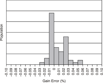
| DC gain error | G = 1 | VOUT = GND + 85 mV to DVDD – 85 mV | 0.006% | 0.1% | ||||
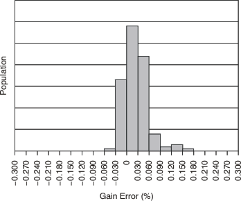
| 1 < G ≤ 32 | VOUT = GND + 85 mV to DVDD – 85 mV | 0.1% | ||||||
| G ≥ 50 | VOUT = GND + 85 mV to DVDD – 85 mV | 0.3% | ||||||
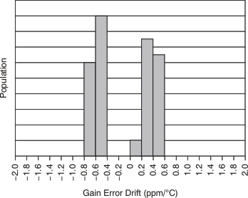
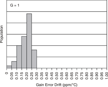
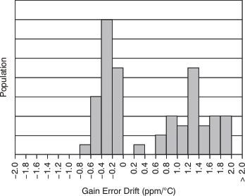
| DC gain drift | G = 1 | VOUT = GND + 85 mV to DVDD – 85 mV | TA = –40°C to 125°C | 0.5 | ppm/°C | |||
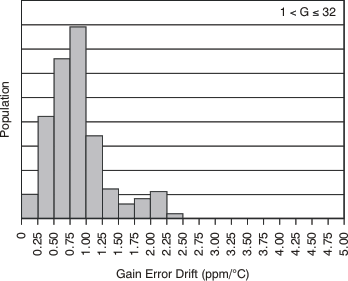
| 1 < G ≤ 32 | VOUT = GND + 85 mV to DVDD – 85 mV | TA = –40°C to 125°C | 2 | ppm/°C | ||||
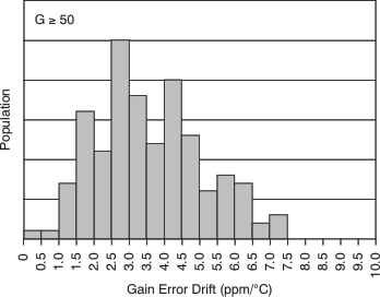
| G ≥ 50 | VOUT = GND + 85 mV to DVDD – 85 mV | TA = –40°C to 125°C | 6 | ppm/°C | ||||
| CAL2 DC gain error(4) | Op Amp + Input = 0.9 VCAL, VREF = VCAL = AVDD/2, G = 1 |
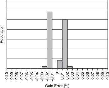
0.02% | ||||||
| CAL2 DC gain drift(4) | Op Amp + Input = 0.9 VCAL, VREF = VCAL = AVDD/2, G = 1 |
TA = –40°C to 125°C | 2 | ppm/°C | ||||
| CAL3 DC gain error(4) | Op Amp + Input = 0.1 VCAL, VREF = VCAL = AVDD/2, G = 1 |
0.02% | ||||||
| CAL3 DC gain drift(4) | Op Amp + Input = 0.1 VCAL, VREF = VCAL = AVDD/2, G = 1 |
TA = –40°C to 125°C | 2 | ppm/°C | ||||
| INPUT IMPEDANCE (CHANNEL OFF)(3) | ||||||||
| Input impedance | CCH | See Figure 55 | 2 | pF | ||||
| INPUT OFF-CHANNEL CURRENT | ||||||||
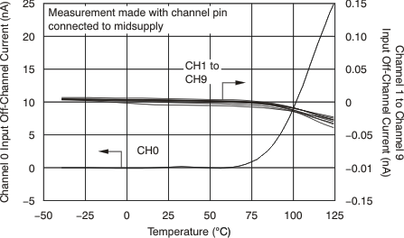
| Input Off-Channel Current (Ch0, Ch1)(5) | ILKG | VREF = GND, VOFF-CHANNEL = AVDD/2, VON-CHANNEL = AVDD/2 – 0.1 V |
±0.05 | ±1 | nA | |||
| Over temperature, –40°C to 125°C | VREF = GND, VOFF-CHANNEL = AVDD/2, VON-CHANNEL = AVDD/2 – 0.1 V |
See Typical Characteristics | ||||||
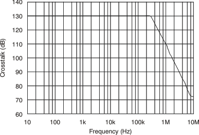
| Channel-to-Channel Crosstalk | 130 | dB | ||||||
| OUTPUT | ||||||||
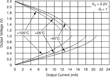
| Voltage output swing from rail | IOUT = ±0.25 mA, AVDD ≥ DVDD(7) | GND + 0.05 | DVDD – 0.05 | V | ||||
| IOUT = ±5 mA, AVDD ≥ DVDD(7) | GND + 0.25 | DVDD – 0.25 | V | |||||
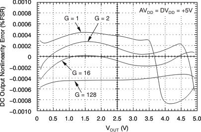
| DC output nonlinearity | VOUT = GND + 85 mV to DVDD – 85 mV(6) | 0.0015 | %FSR | |||||
| Short circuit current | ISC | –30/+60 | mA | |||||
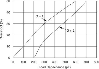
| Capacitive load drive | CLOAD | See Typical Characteristics | ||||||
| NOISE | ||||||||
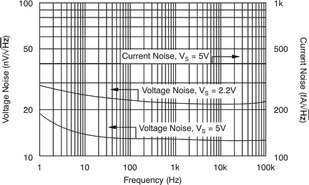
| Input voltage noise density | en | f > 10 kHz, CL = 100 pF, VS = 5 V | 12 | nV/√Hz | ||||
| f > 10 kHz, CL = 100 pF, VS = 2.2 V | 22 | nV/√Hz | ||||||
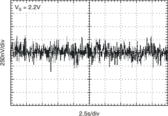
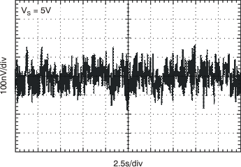
| Input voltage noise | en | f = 0.1 Hz to 10 Hz, CL = 100 pF, VS = 5 V | 0.362 | μVPP | ||||
| f = 0.1 Hz to 10 Hz, CL = 100 pF, VS = 2.2 V | 0.736 | μVPP | ||||||
| Input current density | In | f = 10 kHz, CL = 100 pF | 400 | fA/√Hz | ||||
| SLEW RATE | ||||||||
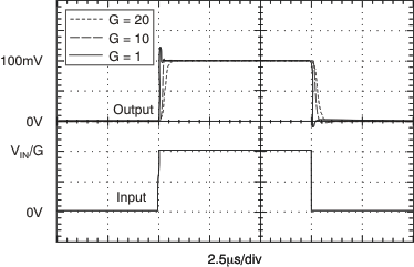
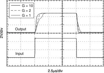
| Slew rate | SR | See Table 1 | V/μs | |||||
| SETTLING TIME | ||||||||
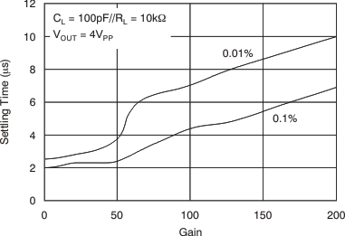
| Settling time | tS | See Table 1 | μs | |||||
| FREQUENCY RESPONSE | ||||||||
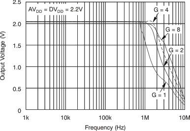
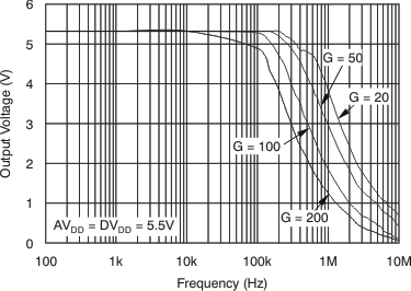
| Frequency response | See Table 1 | MHz | ||||||
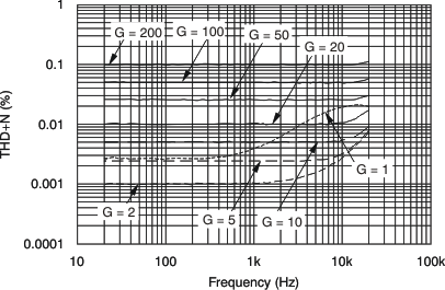
| THD + NOISE | ||||||||
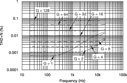
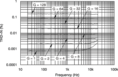
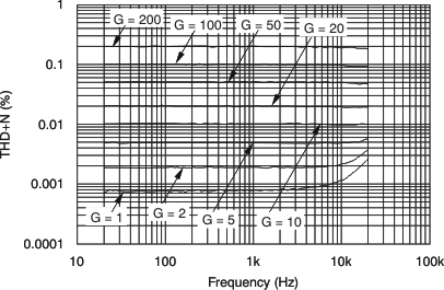
| G = 1, f = 1 kHz, VOUT = 4 VPP at 2.5VDC, CL = 100 pF | 0.003% | |||||||
| G = 10, f = 1 kHz, VOUT = 4 VPP at 2.5VDC, CL = 100 pF | 0.005% | |||||||
| G = 50, f = 1 kHz, VOUT = 4 VPP at 2.5VDC, CL = 100 pF | 0.03% | |||||||
| G = 128, f = 1 kHz, VOUT = 4 VPP at 2.5VDC, CL = 100 pF | 0.08% | |||||||
| G = 200, f = 1 kHz, VOUT = 4 VPP at 2.5VDC, CL = 100 pF | 0.1% | |||||||
| G = 1, f = 20 kHz, VOUT = 4 VPP at 2.5VDC, CL = 100 pF | 0.02% | |||||||
| G = 10, f = 20 kHz, VOUT = 4 VPP at 2.5VDC, CL = 100 pF | 0.01% | |||||||
| G = 50, f = 20 kHz, VOUT = 4 VPP at 2.5VDC, CL = 100 pF | 0.03% | |||||||
| G = 128, f = 20 kHz, VOUT = 4 VPP at 2.5VDC, CL = 100 pF | 0.08% | |||||||
| G = 200, f = 20 kHz, VOUT = 4 VPP at 2.5VDC, CL = 100 pF | 0.11% | |||||||
| POWER SUPPLY | ||||||||
| Operating voltage range(7) | AVDD | 2.2 | 5.5 | V | ||||
| DVDD | 2.2 | 5.5 | V | |||||
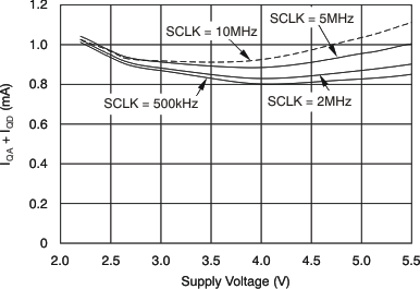
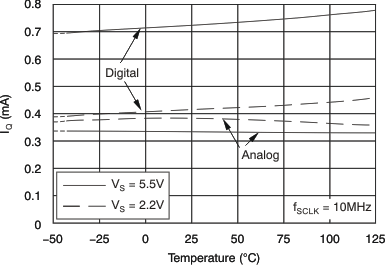
| Quiescent current analog | IQA | IO = 0, G = 1, VOUT = VREF | 0.33 | 0.45 | mA | |||
| Over temperature, –40°C to 125°C | TA = –40°C to 125°C | 0.45 | mA | |||||
| Quiescent current digital(8)(9)(10) | IQD | IO = 0, G = 1, VOUT = VREF, SCLK at 10 MHz, CS = Logic 0, DIO or DIN = Logic 0 |
0.75 | 1.2 | mA | |||
| Over temperature, –40°C to 125°C(8)(9)(10) | IO = 0, G = 1, VOUT = VREF, SCLK at 10 MHz, CS = Logic 0, DIO or DIN = Logic 0 |
TA = –40°C to 125°C | 1.2 | mA | ||||
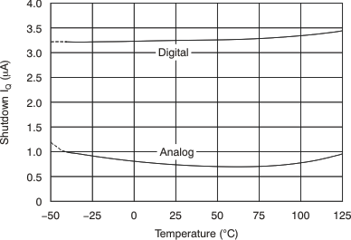
| Shutdown current analog + digital(8)(9) | ISDA + ISDD | IO = 0, VOUT = VREF, G = 1, SCLK Idle | 4 | μA | ||||
| IO = 0, VOUT = 0, G = 1, SCLK at 10MHz, CS = Logic 0, DIO or DIN = Logic 0 |
245 | μA | ||||||
| POWER-ON RESET (POR) | ||||||||
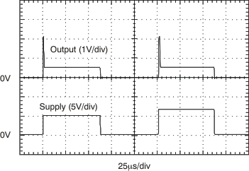
| POR trip voltage | Digital interface disabled and Command Register set to POR values for DVDD < POR Trip Voltage | 1.6 | V | |||||
| TEMPERATURE RANGE | ||||||||
| Specified range | –40 | 125 | °C | |||||
| Operating range | –40 | 125 | °C | |||||
| Thermal resistance | θJA | |||||||
| VSSOP-10 | 164 | °C/W | ||||||
| DIGITAL INPUTS (SCLK, CS, DIO, DIN) | ||||||||
| Logic low | 0 | 0.3DVDD | V | |||||
| Input leakage current (SCLK and CS only) | –1 | 1 | μA | |||||
| Weak pulldown current (DIO, DIN only) | 10 | μA | ||||||
| Logic high | 0.7DVDD | DVDD | V | |||||
| Hysteresis | 700 | mV | ||||||
| DIGITAL OUTPUT (DIO, DOUT) | ||||||||
| Logic high | IOH = –3 mA (sourcing) | DVDD – 0.4 | DVDD | V | ||||
| Logic low | IOL = 3 mA (sinking) | GND | GND + 0.4 | V | ||||
| CHANNEL AND GAIN TIMING | ||||||||
| Channel select time | 0.2 | μs | ||||||
| Gain select time | 0.2 | μs | ||||||
| SHUTDOWN MODE TIMING | ||||||||
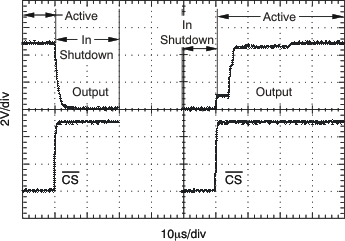
| Enable time | 4 | μs | ||||||
| Disable time | VOUT goes high-impedance, RF and RI remain connected between VOUT and VREF | 2 | μs | |||||
| POWER-ON-RESET (POR) TIMING | ||||||||
| POR power-up time | DVDD ≥ 2 V | 40 | μs | |||||
| POR power-down time | DVDD ≤ 1.5 V | 5 | μs | |||||
(1) Gain error is a function of the input voltage. Gain error outside of the range (GND + 85 mV ≤ VOUT ≤ DVDD – 85 mV) increases to 0.5% (typical).
(2) Input voltages beyond this range must be current-limited to < |10 mA| through the input protection diodes on each channel to prevent permanent destruction of the device.
(3) See Figure 55.
(4) Total VOUT error must be computed using input offset voltage error multiplied by gain. Includes op amp G = 1 error.
(5) Maximum specification limitation limited by final test time and capability.
(6) Measurement limited by noise in test equipment and test time.
(7) When AVDD is less than DVDD, the output is clamped to AVDD + 300 mV.
(8) Does not include current into or out of the VREF pin. Internal RF and RI are always connected between VOUT and VREF.
(9) Digital logic levels: DIO or DIN = logic 0. 10-μA internal pulldown current source.
(10) Includes current from op amp output structure.
7.6 SPI Timing: VS = AVDD = DVDD = 2.2 V to 5 V
At TA = +25°C, RL = 10kΩ//CL = 100pF connected to DVDD/2, and VREF = GND, unless otherwise noted.| MIN | NOM | MAX | UNIT | |||
|---|---|---|---|---|---|---|
| Input capacitance (SCLK, CS, and DIO pins) | 1 | pF | ||||
| tRFI | Input rise and fall time(1)
(CS, SCLK, and DIO pins) |
2 | μs | |||
| tRFO | Output rise and fall time (DIO pin)(1) | CLOAD = 60 pF | 10 | ns | ||
| tCSH | CS high time (CS pin)(1) | 40 | ns | |||
| tCSO | SCLK edge to CS fall setup time(1) | 10 | ns | |||
| tCSSC | CS fall to first SCLK edge setup time | 10 | ns | |||
| fSCLK | SCLK Frequency(2) | 10 | MHz | |||
| tHI | SCLK high time(3) | 40 | ns | |||
| tLO | SCLK low time(3) | 40 | ns | |||
| tSCCS | SCLK last edge to CS rise setup time(1) | 10 | ns | |||
| tCS1 | CS rise to SCLK edge setup time(1) | 10 | ns | |||
| tSU | DIN setup time | 10 | ns | |||
| tHD | DIN hold time | 10 | ns | |||
| tDO | SCLK to DOUT valid propagation delay(1) | 25 | ns | |||
| tSOZ | CS rise to DOUT forced to Hi-Z(1) | 20 | ns | |||
(1) Ensured by design; not production tested.
(2) When using devices in daisy-chain mode, the maximum clock frequency for SCLK is limited by SCLK rise and fall time, DIN setup time, and DOUT propagation delay. See Figure 61. Based on this limitation, the maximum SCLK frequency for daisy-chain mode is 9.09 MHz.
(3) tHI and tLO must not be less than 1/SCLK (maximum).
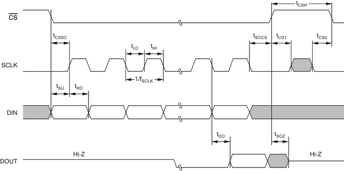 Figure 1. SPI Mode 0, 0
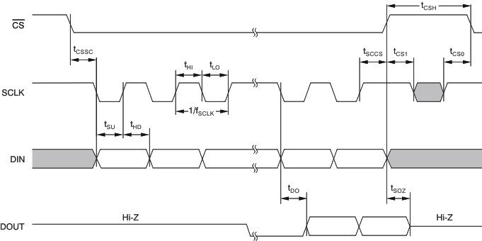 Figure 2. SPI Mode 1, 1
7.7 Typical Characteristics
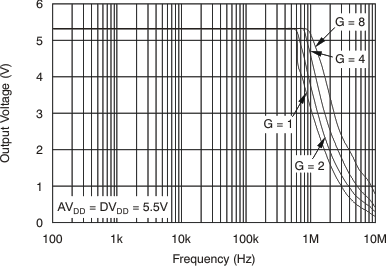
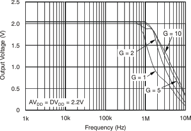
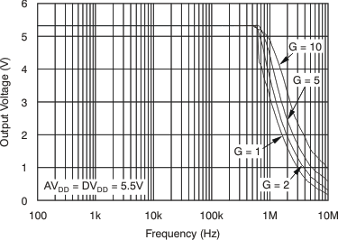
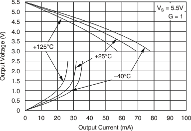
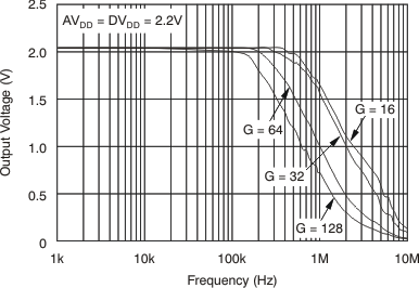
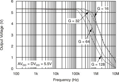
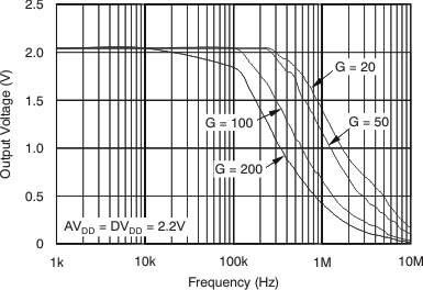
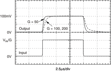
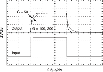
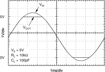
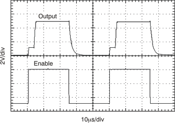
at TA = 25°C, AVDD = DVDD = 5 V, RL = 10 kΩ connected to DVDD/2, VREF = GND, and CL = 100 pF, unless otherwise noted.