ZHCSL30B June 2009 – March 2020 PGA280
PRODUCTION DATA.
- 1 特性
- 2 应用
- 3 说明
- 4 修订历史记录
- 5 Pin Configuration and Functions
- 6 Specifications
-
7 Detailed Description
- 7.1 Overview
- 7.2 Functional Block Diagram
- 7.3 Feature Description
- 7.4 Device Functional Modes
- 7.5 Programming
- 7.6
Register Map
- 7.6.1 Register 0: Gain and External MUX Address (address = 00h) [reset = 0000 0000b]
- 7.6.2 Register 1: Software Reset Register (address = 01h) [reset = 0000 0000b]
- 7.6.3 Register 2: SPI: MODE Selection to GPIO-Pin (address = 02h) [reset = 0000 0000b]
- 7.6.4 Register 3: BUF Timeout Register (address = 03h) [reset = 0001 1001b]
- 7.6.5 Register 4: Error Register (address = 04h) [reset = 0000 0000b]
- 7.6.6 Register 5: GPIO Register (address = 05h) [reset = 0000 0000b]
- 7.6.7 Register 6: Input Switch Control Register 1 (address = 06h) [reset = 0110 0000b]
- 7.6.8 Register 7: Input Switch Control Register 2 (address =07h ) [reset = 0000 0000b]
- 7.6.9 Register 8: GPIO Configuration Register (address = 08h) [reset = 0000 0000b]
- 7.6.10 Register 9: CS Configuration Mode Register (address = 09h) [reset = 0000 0000b]
- 7.6.11 Register 10: Configuration Register 1 (address = 0Ah) [reset = 0000 0000b]
- 7.6.12 Register 11: Configuration Register 2 (address = 0Bh) [reset = 0001 0000b]
- 7.6.13 Register 12: Special Functions Register (address = 0Ch) [reset = 0000 0000b]
- 8 Application and Implementation
- 9 Power Supply Recommendations
- 10器件和文档支持
- 11机械、封装和可订购信息
7.5.2.2.2 GPIO Pin Reference
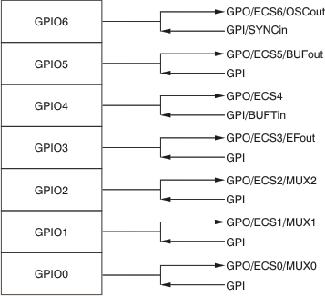
As shown in Figure 54, the PGA280 has seven multi-function pins labeled GPIO0 through GPIO6. These pins can function as general purpose input-output (GPIO) pins either to read a digital input or to output a digital signal as an interrupt or control. GPIO functions are controlled through Register 5 and Register 8.
These pins can also be programmed to have additional special functions for the PGA280. Each of these seven pins can be used as an output for the extended chip select function (ECS), using the PGA280 to redirect the SPI communications to other connected devices. CS Configuration Mode is enabled through Register 9. Additionally, Register 2 controls the clock polarity (CP) of each ECS. For each bit set to 1, a positive edge of SCLK follows CS (CP = 0); for each bit set to 0, a negative edge of SCLK follows CS (CP = 1).
Together with the GPIO and ECS functions, the seven pins can perform more specialized input and output tasks as controlled by Register 12, the Special Functions Register.
GPIO0, GPIO1, and GPIO2 can be used to control an external multiplexer. If the MUX function is enabled in the first three bits of Register 12, the output value on the MUX pins is controlled through Register 0. This configuration allows for simultaneous control of the PGA280 gain and external multiplexer settings by writing to a single register.
GPIO3 can be used to output an error flag. As with bit 3 of Register 4, this option would be the logical OR of the error bits in Register 10 (IARerr, ICAerr, OUTerr, GAINerr, and IOVerr).
GPIO4 can be used as an input to trigger the current buffer. The low-to-high edge of a pulse starts the buffer with a delay of three to four clock cycles. If held high, the buffer [BUFA] remains active. The active time is extended by a minimum of three to four clock cycles in addition to the time set with FLAGTIM.
GPIO5 can be configured as an output to indicate a buffer active condition. The polarity is controlled by BUFApol of bit 5 in Register 10.
GPIO6 can be configured as either an output or an input with the Special Functions Register. With Bit 7, OSCOUT connects the internal oscillator to GPIO6. With Bit 6, SYNCIN allows an external oscillator to provide the master clock to the PGA280.
To use any of these functions, Register 8 must first be set to 0 for input or to 1 for an output (for GPIO, ECS, or special function).
Once set, any 1s in Register 9 supersede the GPIO function for the related pin, allowing for CS configuration.
Likewise, any 1s in Register 12 supersede the GPIO function and CS configuration, allowing for any of the pin-specific special functions to operate.
 Figure 54. Special Function to Pin Assignment Reference