ZHCSL30B June 2009 – March 2020 PGA280
PRODUCTION DATA.
- 1 特性
- 2 应用
- 3 说明
- 4 修订历史记录
- 5 Pin Configuration and Functions
- 6 Specifications
-
7 Detailed Description
- 7.1 Overview
- 7.2 Functional Block Diagram
- 7.3 Feature Description
- 7.4 Device Functional Modes
- 7.5 Programming
- 7.6
Register Map
- 7.6.1 Register 0: Gain and External MUX Address (address = 00h) [reset = 0000 0000b]
- 7.6.2 Register 1: Software Reset Register (address = 01h) [reset = 0000 0000b]
- 7.6.3 Register 2: SPI: MODE Selection to GPIO-Pin (address = 02h) [reset = 0000 0000b]
- 7.6.4 Register 3: BUF Timeout Register (address = 03h) [reset = 0001 1001b]
- 7.6.5 Register 4: Error Register (address = 04h) [reset = 0000 0000b]
- 7.6.6 Register 5: GPIO Register (address = 05h) [reset = 0000 0000b]
- 7.6.7 Register 6: Input Switch Control Register 1 (address = 06h) [reset = 0110 0000b]
- 7.6.8 Register 7: Input Switch Control Register 2 (address =07h ) [reset = 0000 0000b]
- 7.6.9 Register 8: GPIO Configuration Register (address = 08h) [reset = 0000 0000b]
- 7.6.10 Register 9: CS Configuration Mode Register (address = 09h) [reset = 0000 0000b]
- 7.6.11 Register 10: Configuration Register 1 (address = 0Ah) [reset = 0000 0000b]
- 7.6.12 Register 11: Configuration Register 2 (address = 0Bh) [reset = 0001 0000b]
- 7.6.13 Register 12: Special Functions Register (address = 0Ch) [reset = 0000 0000b]
- 8 Application and Implementation
- 9 Power Supply Recommendations
- 10器件和文档支持
- 11机械、封装和可订购信息
5 Pin Configuration and Functions
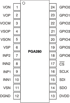
TSSOP-24
PW PACKAGE
(TOP VIEW)

Pin Functions
| PIN | DESCRIPTION | PIN | DESCRIPTION | |||
|---|---|---|---|---|---|---|
| NO. | NAME | NO. | NAME | |||
| 1 | VON | Inverting signal output | 13 | DVDD | Digital supply | |
| 2 | VOP | Noninverting signal output | 14 | SDO | SPI slave data output | |
| 3 | VOCM | Input, output common-mode voltage | 15 | SDI | SPI slave data input | |
| 4 | VSOP | Positive supply for output | 16 | SCLK | SPI clock input | |
| 5 | VSON | Negative supply for output, AGND | 17 | CS | SPI chip select input; active low | |
| 6 | VSP | Positive high-voltage supply | 18 | GPIO6 | GPIO 6, SYNC (in), OSC (out), ECS6 | |
| 7 | INP2 | AUX input, noninverting | 19 | GPIO5 | GPIO 5, BUFA (out), ECS5 | |
| 8 | INN2 | AUX input, inverting | 20 | GPIO4 | GPIO 4, BUFT (in), ECS4 | |
| 9 | INP1 | Signal input, noninverting | 21 | GPIO3 | GPIO 3, EF (out), ECS3 | |
| 10 | INN1 | Signal input, inverting | 22 | GPIO2 | GPIO 2, ECS2, MUX2 | |
| 11 | VSN | Negative high-voltage supply | 23 | GPIO1 | GPIO 1, ECS1, MUX1 | |
| 12 | DGND | Digital ground | 24 | GPIO0 | GPIO 0, ECS0, MUX0 | |