ZHCSL30B June 2009 – March 2020 PGA280
PRODUCTION DATA.
- 1 特性
- 2 应用
- 3 说明
- 4 修订历史记录
- 5 Pin Configuration and Functions
- 6 Specifications
-
7 Detailed Description
- 7.1 Overview
- 7.2 Functional Block Diagram
- 7.3 Feature Description
- 7.4 Device Functional Modes
- 7.5 Programming
- 7.6
Register Map
- 7.6.1 Register 0: Gain and External MUX Address (address = 00h) [reset = 0000 0000b]
- 7.6.2 Register 1: Software Reset Register (address = 01h) [reset = 0000 0000b]
- 7.6.3 Register 2: SPI: MODE Selection to GPIO-Pin (address = 02h) [reset = 0000 0000b]
- 7.6.4 Register 3: BUF Timeout Register (address = 03h) [reset = 0001 1001b]
- 7.6.5 Register 4: Error Register (address = 04h) [reset = 0000 0000b]
- 7.6.6 Register 5: GPIO Register (address = 05h) [reset = 0000 0000b]
- 7.6.7 Register 6: Input Switch Control Register 1 (address = 06h) [reset = 0110 0000b]
- 7.6.8 Register 7: Input Switch Control Register 2 (address =07h ) [reset = 0000 0000b]
- 7.6.9 Register 8: GPIO Configuration Register (address = 08h) [reset = 0000 0000b]
- 7.6.10 Register 9: CS Configuration Mode Register (address = 09h) [reset = 0000 0000b]
- 7.6.11 Register 10: Configuration Register 1 (address = 0Ah) [reset = 0000 0000b]
- 7.6.12 Register 11: Configuration Register 2 (address = 0Bh) [reset = 0001 0000b]
- 7.6.13 Register 12: Special Functions Register (address = 0Ch) [reset = 0000 0000b]
- 8 Application and Implementation
- 9 Power Supply Recommendations
- 10器件和文档支持
- 11机械、封装和可订购信息
9 Power Supply Recommendations
The PGA280 can connect to three supply voltages: the high-voltage analog supply, the low-voltage output amplifier supply, and the digital I/O supply. This architecture allows an optimal interface (level-shift) to the different supply domains.
The high-voltage analog supply, VSP and VSN, powers the high-voltage input section. The substrate of the IC is connected to VSN; therefore, VCN must be connected to the most negative potential.
The low-voltage analog output supply, VSOP and VSON, can operate within the high-voltage supply boundaries with two minimal limitations:
- The usable range for VSON is from a minimum 5 V below VSP to as low as VSN. This 5 V provides the headroom for the output supply voltage of 2.7 V to 5 V. Even with less than 5V supply, this voltage difference is required for proper operation.
- The common-mode control input, VOCM, requires a voltage at least 2 V from VSP, in order to support internal rail-to-rail performance.
These limits may only come into consideration when using a minimum supply or an extremely asymmetrical high-voltage supply. In most practical cases, VSON is connected to the ground of the system 3-V or 5-V supply.
VSOP can be turned on first or can be higher than VSP without harm, but operation fails if VSP and VSN are not present.
Observe the maximum voltage applied between VSOP and VSON, because there is no internal protection. This consideration is the same as with other standard operational amplifier devices.
The digital supply, DGND and DVDD, can also be set within the boundaries of VSP and VSN. Only the positive supply, DVDD, cannot be closer than 1 V less than VSP. DVDD can be turned on without the analog supply being present and is operational, but limited to digital functions in this case. The maximum supply voltage must be observed because there is no internal protection. VSOP and VSON can be connected with DVDD and DGND, if desired.
Current consumption of the digital supply is very low under static conditions, but increases with communications activity. Assuming no external load except the 20 pF load to SDO, with an SCLK = 10 MHz and a 3-V supply, the current momentarily increases by approximately 0.6 mA when reading a register. With a 5-V digital supply, the increase is in the range of 0.8 mA. This additional current is only required during communication; a larger bypass capacitor can supply this current. Driving current into SDO would further increase the current demand.
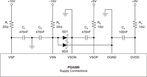
VSN is connected to the substrate; therefore, the voltage at VSON or DGND must not turn on the substrate diode to VSN. Use external Schottky diodes from VSON to VSN and from DGND to VSN (see Figure 70) to prevent such a condition.
The PGA280 uses an internal chopper technology, and therefore works best with good supply decoupling. Series resistors in the supply are recommended to build an RC low-pass filter. With the small supply current, these series resistors can be in the range of 15 Ω to 22 Ω. The RC filter also prevents a very fast rise time of the supply voltage, thus avoiding parasitic currents in the device. Connecting supply wires into an already-turned on supply (very fast rise time) without such a filter can damage the device as a result of voltage overshoot and parasitic charge currents. Figure 70 shows an example of a supply connection using RC bypass filters. DVDD may not need decoupling, but if the digital supply is noisy, a filter is recommended at C4 and R4.
NOTE
Rise and fall times for the high-voltage supplies must be slower than 1 V/μs.

NOTE:
In this example, the Schottky diodes prevent substrate reversing. The supply voltages shown are only example values.