ZHCS861B April 2012 – June 2015 PGA450-Q1
PRODUCTION DATA.
- 1 特性
- 2 应用
- 3 说明
- 4 修订历史记录
- 5 Pin Configuration and Functions
-
6 Specifications
- 6.1 Absolute Maximum Ratings
- 6.2 ESD Ratings
- 6.3 Recommended Operating Conditions
- 6.4 Thermal Information
- 6.5 Electrical Characteristics
- 6.6 Electrical Characteristics — LIN 2.1 Slave and Buffered SCI
- 6.7 Electrical Characteristics — SPI Interface
- 6.8 Timing Requirements
- 6.9 Timing Requirements — LIN 2.1 Slave and Buffered SCI
- 6.10 Timing Requirements — SPI Interface
- 6.11 Switching Characteristics
- 6.12 Digital Datapath Filter Switching Characteristics
- 6.13 Typical Characteristics
-
7 Detailed Description
- 7.1 Overview
- 7.2 Functional Block Diagram
- 7.3
Feature Description
- 7.3.1 Power Supply Block
- 7.3.2 VREG
- 7.3.3 Clock
- 7.3.4 Low-Side Drive FETs
- 7.3.5 Burst Generator
- 7.3.6 Low-Noise Amplifier
- 7.3.7 Analog-to-Digital Converter
- 7.3.8 Digital Data Path
- 7.3.9 Transducer Saturation Time
- 7.3.10 Temperature Sensor
- 7.3.11 Free-Running Timer
- 7.3.12 GPIOs
- 7.3.13 8051W UART
- 7.3.14 8051 WARP Core
- 7.3.15 Memory
- 7.3.16
LIN 2.1 Slave and Buffered SCI
- 7.3.16.1 Physical Layer
- 7.3.16.2 LIN Slave Mode
- 7.3.16.3 SCI Buffered Mode
- 7.3.16.4 Connection of LIN Pin to 8051W
- 7.4 Device Functional Modes
- 7.5
Programming
- 7.5.1 SPI Interface
- 7.5.2 Diagnostics
- 7.5.3 8051W Interrupts
- 7.5.4 Instructions
- 7.5.5 8051W Port Usage
- 7.6
Register Maps
- 7.6.1
SFR Registers
- 7.6.1.1 I/O Ports (P0, P1, P2, P3) Registers
- 7.6.1.2 Stack Pointer Register (offset = 0x81) [reset = 0]
- 7.6.1.3 Data Pointer Registers
- 7.6.1.4 Power Control Register (offset = 0x87) [reset = 0]
- 7.6.1.5 Timer and Counter Control Register (offset = 0x88) [reset = 0]
- 7.6.1.6 Timer and Counter Mode Register (offset = 0x89) [reset = 0]
- 7.6.1.7 Timer and Counter Data Registers (TL0, TL1, TH0, TH1)
- 7.6.1.8 UART Control Register (offset = 0x98) [reset = 0]
- 7.6.1.9 UART Data Register (offset = 0x99) [reset = 0]
- 7.6.1.10 Interrupt Enable Register 0 (offset = 0xA8) [reset = 0]
- 7.6.1.11 Interrupt Enable Register 1 (offset = 0xE8) [reset = 0]
- 7.6.1.12 Interrupt Priority Register 0 (offset = 0xB8) [reset = 0]
- 7.6.1.13 Interrupt Priority Register 1 (offset = 0xF8) [reset = 0]
- 7.6.1.14 Program Status Word Register (offset = 0xD0) [reset = 0]
- 7.6.1.15 Accumulator Register (offset = 0xE0) [reset = 0]
- 7.6.1.16 B Register (offset = 0xF0) [reset = 0]
- 7.6.2
ESFR Registers
- 7.6.2.1 Bandpass Filter Coefficient B1 (BPF_B1) Register
- 7.6.2.2 Bandpass Filter Coefficient A2 (BPF_A2) Registers
- 7.6.2.3 Band-Pass Filter Coefficient A3 (BPF_A3) Register
- 7.6.2.4 Low-Pass Filter Coefficient B1 (LPF_B1) Registers
- 7.6.2.5 Low-Pass Filter Coefficient A2 (LPF_A2) Registers
- 7.6.2.6 Downsample Register (offset = 0xA5) [reset = 0]
- 7.6.2.7 BURST ON A Duration (ON_A) Registers
- 7.6.2.8 BURST OFFA Duration (OFF_A) Register
- 7.6.2.9 BURST ON B Duration (ON_B) Registers
- 7.6.2.10 BURST OFF B Duration (OFF_B) Register
- 7.6.2.11 Pulse Count A Register (offset = 0xAF) [reset = 0]
- 7.6.2.12 Pulse Count B Register (offset = 0xB1) [reset = 0]
- 7.6.2.13 Deadtime Register (offset = 0xB2) [reset = 0]
- 7.6.2.14 Burst Mode Register (offset = 0xB3) [reset = 0]
- 7.6.2.15 Temperature Sensor Register (offset = 0xB4) [reset = 0]
- 7.6.2.16 Saturation Deglitch Time Register (offset = 0xB5) [reset = 0]
- 7.6.2.17 Saturation Time Capture Register (offset = 0xB6) [reset = 0]
- 7.6.2.18 Control 1 Register (offset = 0xB7) [reset = 0]
- 7.6.2.19 Blanking Timer Register (offset = 0xB9) [reset = 0]
- 7.6.2.20 Free Running Timer (FRT) Registers
- 7.6.2.21 GPIO Control Register (offset = 0xBC) [reset = 0]
- 7.6.2.22 Clock Select Register (offset = 0xBD) [reset = 0]
- 7.6.2.23 Watchdog Enable Register (offset = 0xBE) [reset = 0]
- 7.6.2.24 LIN/SCI Select Register (offset = 0xBF) [reset = 0]
- 7.6.2.25 EEPROM Control Register (offset = 0xC0) [reset = 0]
- 7.6.2.26 Status 1 (STATUS1) Register (offset = 0xC1) [reset = 0]
- 7.6.2.27 Status 2 Register (offset = 0xC2) [reset = 0]
- 7.6.2.28 Power Mode Register (offset = 0xC3) [reset = 0]
- 7.6.2.29 Datapath and SCI Control Register (offset = 0xC4) [reset = 0]
- 7.6.2.30 FIFO Control Register (offset = 0xC5) [reset = ]
- 7.6.2.31 Enable Control Register (offset = 0xC8) [reset = 0]
- 7.6.2.32 LIN/SCI Rx Data (RX_DATAx) Register (offset = 0xC9 to 0xD1) [reset = 0]
- 7.6.2.33 LIN PID Register (offset = 0xD2) [reset = 0]
- 7.6.2.34 LIN/SCI Tx Data Registers (offset = 0xD3 to 0xDA) [reset = 0]
- 7.6.2.35 LIN/SCI Data Count Register (offset = 0xDB) [reset = 0]
- 7.6.2.36 LIN Configuration Register (offset = 0xDC) [reset = 0x40]
- 7.6.2.37 LIN Control Register (offset = 0xDD) [reset = 0]
- 7.6.2.38 LIN STATUS Register (offset = 0xDE) [reset = 0]
- 7.6.2.39 FIFO Pointer (FIFO_POINTER) Registers
- 7.6.2.40 VREG Select Register (offset = 0xE2) [reset = 0]
- 7.6.2.41 Sync Count (SYNC_COUNT) Registers
- 7.6.2.42 TEMP/DAC Control Register (offset = 0xE5) [reset = 0]
- 7.6.2.43 Oscillator Sync Control Register (offset = 0xE6) [reset = 0]
- 7.6.3 TEST Registers
- 7.6.1
SFR Registers
- 8 Application and Implementation
- 9 Power Supply Recommendations
- 10Layout
- 11器件和文档支持
- 12机械、封装和可订购信息
6 Specifications
6.1 Absolute Maximum Ratings
over operating free-air temperature range (unless otherwise noted)(1)| MIN | MAX | UNIT | ||
|---|---|---|---|---|
| Power-supply voltage | VPWR | –0.3 | 40 | V |
| Voltage | VREG, VPROG_OTP pin | –0.3 | 10 | V |
| LIN | –27 | 40 | V | |
| RBIAS, CIN, IN | –0.3 | 3 | V | |
| DVDD, XIN, XOUT | –0.3 | 2 | V | |
| OUTA, OUTB | –0.3 | 40 | V | |
| LIM | –1.5 | 1.5 | V | |
| Voltage on all other pins, VMAX | –0.3 | 6 | V | |
| Low-side FET current, IFET | 1.5 | A | ||
| Maximum operating junction temperature, TJmax | –40 | 150 | ℃ | |
| Storage temperature, Tstg | –40 | 125 | °C | |
(1) Stresses beyond those listed under Absolute Maximum Ratings may cause permanent damage to the device. These are stress ratings only and functional operation of the device at these or any other conditions beyond those indicated under Recommended Operating Conditions are not implied. Exposure to Absolute-Maximum-Rated conditions for extended periods may affect device reliability.
6.2 ESD Ratings
| VALUE | UNIT | ||||
|---|---|---|---|---|---|
| V(ESD) | Electrostatic discharge | Human body model (HBM), per AEC Q100-002(1) | ±2000 | V | |
| IEC61000-4–2(2) | LIN pin | ±8000 | |||
| Charged device model (CDM), per AEC Q100-011 | Corner pins (1, 14, 15, and 28) | ±750 | |||
| Other pins | ±500 | ||||
(1) AEC Q100-002 indicates HBM stressing is done in accordance with the ANSI/ESDA/JEDEC JS-001 specification.
(2) Per IEC61000-4–2:1995 specification, contact with no external capacitor.
6.3 Recommended Operating Conditions
over operating free-air temperature range (unless otherwise noted)| MIN | NOM | MAX | UNIT | |||
|---|---|---|---|---|---|---|
| VPWR | Power-supply voltage | 7 | 18 | V | ||
| IPWR | Power-supply current | Power up, TA = 105°C | 50 | mA | ||
| Active mode(1) temperature sensor off, TA = 105°C, VPWR = 18 V | 15 | mA | ||||
| Quiet mode(1), TA = 105°C, VPWR = 18 V | 7.5 | mA | ||||
| IPWRAVG | Average power-supply current(1) | 10 | mA | |||
| TA | Operating ambient temperature | –40 | 105 | ℃ | ||
| CVREG | Capacitance on VREG pin | 10 | 470 | µF | ||
| CVPWR | Capacitance on VPWR pin(2) | 47 | 100 | µF | ||
| CESR | ESR of capacitor on VREG pin | 2 | Ω | |||
(1) The average current is defined as: Ipwr(Average) = 0.3Iactive + 0.7Iquiet
Active Mode: The entire device is active.
Quiet Mode: LNA, A/D, digital datapath, and OUTA/B are OFF. Microprocessor and LIN are still active. Add 100 mA to these currents if capacitor on VREG is charging
Active Mode: The entire device is active.
Quiet Mode: LNA, A/D, digital datapath, and OUTA/B are OFF. Microprocessor and LIN are still active. Add 100 mA to these currents if capacitor on VREG is charging
(2) The capacitor value must allow a discharge rate on VPWR to be at most 1 V/ms.
6.4 Thermal Information
| THERMAL METRIC(1) | PGA450-Q1 | UNIT | |
|---|---|---|---|
| PWP (TSSOP) | |||
| 28 PINS | |||
| RθJA | Junction-to-ambient thermal resistance | 68.7 | °C/W |
| RθJC | Junction-to-case (top) thermal resistance | 11.6 | °C/W |
| RθJB | Junction-to-board thermal resistance | 27.6 | °C/W |
(1) For more information about traditional and new thermal metrics, see the Semiconductor and IC Package Thermal Metrics application report, SPRA953.
6.5 Electrical Characteristics
| PARAMETER | TEST CONDITIONS | MIN | TYP | MAX | UNIT | ||
|---|---|---|---|---|---|---|---|
| POWER SUPPLY | |||||||
| VPWRPOR | VPWR voltage for POR to occur | POR is deasserted | 3 | 4.2 | V | ||
| VAVDD | AVDD pin voltage | IAVDD = 5 mA | 4.75 | 5 | 5.25 | V | |
| IAVDD | AVDD pin load current | 5 | mA | ||||
| VDVDD | DVDD pin voltage | 1.8 | V | ||||
| VREF | VREF pin voltage | 3 | V | ||||
| VREG | |||||||
| VREGTOL | Transducer primary voltage tolerance | IREG = 100 µA | VPWR = 7 V VREG_SEL = 0_XXX for 4.7 V–5.4 V |
±100 | mV | ||
| VPWR = 10 V VREG_SEL = 1_XXX for 7.7 V–8.4 V |
±150 | ||||||
| VREGCHARGE | Transducer voltage droop while charging | IREG = 100 mA, below VREG_SEL setting | 500 | mV | |||
| VREGREADY | VREG_READY threshold | Below VREG_SEL setting | 250 | ||||
| IVREG | VREG output current | VPWR > VREG_SEL + 2.5 V | 90 | 100 | 110 | mA | |
| VPWR > VREG_SEL + 2 V | 100 | µA | |||||
| VREGI_S2G | VREG short-to-ground protection current | VPWR = 16 V, TA = 105 °C, no burst | 110 | mA | |||
| LOW-SIDE DRIVE MOSFETS | |||||||
| rds(on) | FET ON resistance | Iload = 500 mA, TA = 105 °C | 1.2 | Ω | |||
| IPULSE | Drain pulse current | 50 kHz | 1.5 | A | |||
| Drive clamping voltage | Vgs = 0 V, Idd = 10 mA | 40 | V | ||||
| Leakage current | 5 | µA | |||||
| LOW NOISE AMPLIFIER | |||||||
| AV | Gain | LNA_GAIN setting = 0b00 | 1680 | 1750 | 1820 | V/V | |
| LNA_GAIN setting = 0b01 | 892 | 930 | 968 | ||||
| LNA_GAIN Setting = 0b10 | 496 | 517 | 538 | ||||
| LNA_GAIN Setting = 0b11 | 99 | 104 | 109 | ||||
| RIN | Input impedance | 40 kHz | 100 | kΩ | |||
| Clamp voltage | –1.5 | 1.5 | V | ||||
| ILIM | Input current limit | 200 | mA | ||||
| Noise (input-referred of the signal chain) | IN pin = GND, TA = 105 °C, center frequency = 40 kHz, Bandwidth = 10 kHz | 0.7 | µVrms | ||||
| Input-referred PSRR | VPWR = 7 V, LNA gain setting = 0b00 | 93 | dB | ||||
| 12-BIT ADC | |||||||
| VADCREF | Input voltage range | 0 | 3 | V | |||
| DNL | 20% to 80% input range | 2.5 | LSB | ||||
| INL | 20% to 80% input range, best-fit curve | 4 | LSB | ||||
| Gain | Best-fit curve | 1373 | 1378 | 1383 | LSB/V | ||
| Offset | Best-fit curve | –15 | LSB | ||||
| 8-BIT DAC | |||||||
| VDAC_MAX | Output range | 0.133 | 1.125 | V | |||
| Gain | 3.9 | mV/Code | |||||
| Offset voltage | Output when DAC code is 000h at Rload = 100 kΩ to GND | 0.133 | V | ||||
| Full-scale voltage | Output when DAC code is 0xFF Rload = 100 kΩ to GND | 1.125 | V | ||||
| IDAC | Output current | DAC Code = 0x00 DAC Code = 0xFF, Rload = 100 kΩ |
12.5 | µA | |||
| INL | –2 | 2 | LSB | ||||
| DNL | –1 | 1 | LSB | ||||
| Capacitance load | 10 | pF | |||||
| TRANSDUCER SATURATION TIME | |||||||
| VSAT_TH | Saturation threshold | SAT_SEL = 200 mV | 200 | mV | |||
| SAT_SEL = 300 mV | 300 | mV | |||||
| SAT_SEL = 400 mV | 400 | mV | |||||
| SAT_SEL = 600 mV | 600 | mV | |||||
| TEMPERATURE SENSOR | |||||||
| Temperature sensor range | –40 | 140 | °C | ||||
| Temperature accuracy | –40°C to 105°C | –5 | 5 | °C | |||
| Temperature sensor code | 30°C | 0 | LSB | ||||
| Temperature sensor LSB | 1.75 | °C/LSB | |||||
| GPIOS, 8051 UART Tx AND Rx | |||||||
| VIH | GPIO input mode, high, Rx, | Rload > 10 kΩ | 3.5 | 5.3 | V | ||
| VIL | GPIO input mode, low, Rx | –0.3 | 1.5 | V | |||
| RPULLUP | Internal pullup on input | Pullup is to AVDD | 100 | KΩ | |||
| VOH | GPIO strong-mode output, high, Tx | IOH = 5 mA | 4 | V | |||
| VOL | GPIO strong-mode output, low, Tx | IOL = 5 mA | 0.8 | V | |||
| Total current on GPIO1 + GPIO2 +Tx pin | No load on AVDD pin | 5 | mA | ||||
| MEMORY | |||||||
| OTP programming voltage | 7.5 | 8 | 8.5 | V | |||
| OTP programming current | 2 | 5 | mA | ||||
| DIAGNOSTICS | |||||||
| VPWR_OV | VPWR overvoltage level | 25 | 28 | 32 | V | ||
| AVDD_UV | VPWR for AVDD undervoltage | 5.6 | V | ||||
| AVDD_OC | AVDD Overcurrent | 45 | 55 | 65 | mA | ||
| RBIAS_OC | RBIAS Overcurrent | 65 | 80 | 90 | µA | ||
| Low-side driver A/B drain monitor | 2.2 | 2.5 | 2.8 | V | |||
| Low-side driver A/B monitor | 2.2 | 2.5 | 2.8 | V | |||
| Over temperature shut-off protection | 150 | 200 | ℃ | ||||
6.6 Electrical Characteristics — LIN 2.1 Slave and Buffered SCI(1)(2)
| PARAMETER | TEST CONDITIONS | MIN | TYP | MAX | UNIT |
|---|---|---|---|---|---|
| IBUS_LIM |
V BUS= 18 V |
40 | 200 | mA | |
| IBUS_PAS_dom | Driver off, VBUS= 0V, VPWR= 12 V | –1 | mA | ||
| IBUS_PAS_rec | Driver off, 7 V < VPWR < 18 V, 8 V < VBUS < 18 V, VBUS > VPWR | 20 | µA | ||
| IBUS_NO_GND | GNDDevice = V PWR, 0 < VBUS < 18 V, VPWR = 12 V | –1 | 1 | mA | |
| IBUS_NO_BAT | V PWR= GND, 0 < V BUS < 18 V | 100 | µA | ||
| VBUSdom | Receiver dominant state | 0.4 | VPWR | ||
| VBUSrec | Receiver recessive state | 0.6 | VPWR | ||
| VBUS_CNT | VBUS_CNT = (V th_dom+ V th_rec)/2 | 0.475 | 0.5 | 0.525 | VPWR |
| VHYS | VHYS = Vth_rec – Vth_dom | 0.175 | VPWR | ||
| RSlave | Serial resistor | 20 | 30 | 60 | KΩ |
| CIN | Input capacitance on LIN pin | 60 | pF |
(1) LIN Mode:
LIN 2.1 physical layer and LIN protocol (Section 2.1 of LIN 2.1) specification
Exceptions: No wake-up (Section 2.6.2 of LIN 2.1)
No transport layer in digital logic (Section 3 of LIN 2.1)
No node configuration and identification services in digital (Section 4 of LIN 2.1)
No diagnostic layer in digital logic (Section 5 of LIN 2.1)
The device is not certified for LIN compliance. Communication baud rate is fixed at 19.2 kBPS.
(2) SCI Mode:
None
None
6.7 Electrical Characteristics — SPI Interface
| PARAMETER | TEST CONDITIONS | MIN | TYP | MAX | UNIT | |
|---|---|---|---|---|---|---|
| High-level voltage (CS, SCK, SDI, SDO) | 3.5 | V | ||||
| Low-level voltage (CS, SCK, SDI, SDO) | 1.5 | V | ||||
| CL(SDO) | Capacitive load for data output (SDO) | 10 | pF | |||
6.8 Timing Requirements
6.9 Timing Requirements — LIN 2.1 Slave and Buffered SCI(1)(2)
Figure 1 shows the LIN timing details.| MIN | NOM | MAX | UNIT | ||
|---|---|---|---|---|---|
| D1 | THRec(max) = 0.744 × VPWR; THDom(max) = 0.581 × V PWR; V PWR= 7 V...18 V; tBit= 50 µs; D1 = tBus_rec(min)/ (2 × tBit) Load1; CBUS = 1 nF; RBUS = 1KΩ Load2; CBUS = 6.8 nF; RBUS = 660 Ω Load3: CBUS = 10 nF; RBUS = 500 Ω, see Figure 1. |
0.396 | |||
| D2 | THRec(min)= 0.522 × VPWR; THDom(min) = 0.284 × VPWR; VPWR= 7.6 V...18 V; tBit = 50 µs; D2 = tBus_rec(max)/ (2 × t Bit) Load1; CBUS = 1 nF; RBUS = 1 kΩ Load2; CBUS = 6.8 nF; R BUS = 660 Ω Load3; C BUS=10 nF; RBUS = 500 Ω, see Figure 1. |
0.581 | |||
| D3 | THRec(max) = 0.778 × VPWR; THDom(max) = 0.616 × V PWR; V PWR= 7 V to 18 V; tBit = 96 µs; D4 = tBus_rec(min) / (2 × t Bit) Load1; C BUS = 1 nF; RBUS = 1 kΩ Load2; CBUS = 6.8 nF; RBUS = 660 Ω Load3; CBUS = 10 nF; RBUS = 500 Ω, see Figure 1. |
0.417 | |||
| D4 | THRec(min) = 0.389 × VPWR; THDom(min) = 0.251 × VPWR; VPWR = 7.6 V to 18 V; tBit= 96 µs; D4 = tBus_rec(max) / (2 × t Bit) Load1; CBUS = 1 nF; RBUS = 1 kΩ Load2; CBUS = 6.8 nF; RBUS = 660 Ω Load3; CBUS = 10 nF; RBUS = 500 Ω, see Figure 1. |
0.590 | |||
| trx_pd | Propagation delay of receiver RRXD = 2.4 kΩ; CRXD = 20 pF |
6 | µs | ||
| trx_sym | Symmetry of receiver propagation delay rising edge with respect to falling edge RRXD = 2.4 kΩ; C RXD = 20 pF |
–2 | 2 | µs | |
(1) LIN Mode:
LIN 2.1 physical layer and LIN protocol (Section 2.1 of LIN 2.1) specification
Exceptions: No wake-up (Section 2.6.2 of LIN 2.1)
No transport layer in digital logic (Section 3 of LIN 2.1)
No node configuration and identification services in digital (Section 4 of LIN 2.1)
No diagnostic layer in digital logic (Section 5 of LIN 2.1)
The device is not certified for LIN compliance. Communication baud rate is fixed at 19.2 kBPS.
LIN 2.1 physical layer and LIN protocol (Section 2.1 of LIN 2.1) specification
Exceptions: No wake-up (Section 2.6.2 of LIN 2.1)
No transport layer in digital logic (Section 3 of LIN 2.1)
No node configuration and identification services in digital (Section 4 of LIN 2.1)
No diagnostic layer in digital logic (Section 5 of LIN 2.1)
The device is not certified for LIN compliance. Communication baud rate is fixed at 19.2 kBPS.
(2) SCI Mode:
None
None
6.10 Timing Requirements — SPI Interface
Figure 2 shows the SPI clocking details.| MIN | NOM | MAX | UNIT | |||
|---|---|---|---|---|---|---|
| fSCK | SPI frequency | 8 | MHz | |||
| tCSSCK | CS low to first SCK rising edge | See Figure 2. | 125 | ns | ||
| tSCKCS | Last SCK rising edge to CS rising edge | 125 | ns | |||
| tCSD | CS disable time | 375 | ns | |||
| tDS | SDI setup time | 25 | ns | |||
| tDH | SDI hold time | 25 | ns | |||
| tSDIS | SDI fall/rise time | 25 | ns | |||
| tSCKR | SCK rise time | 7 | ns | |||
| tSCKF | SCK fall time | 7 | ns | |||
| tSCKH | SCK high time | 62.5 | ns | |||
| tSCKL | SCK low time | 62.5 | ns | |||
| tSDO | SDO enable time | 25 | ns | |||
| tACCS | SCK rising edge to SDO data valid | 25 | ns | |||
| tSDOD | SDO disable time | 25 | ns | |||
| tSDOS | SDO rise/fall time | CSDO = 10 pF, see Figure 2. | 1 | 15 | ns | |
6.11 Switching Characteristics
over operating free-air temperature range (unless otherwise noted)| PARAMETER | TEST CONDITIONS | MIN | TYP | MAX | UNIT | |
|---|---|---|---|---|---|---|
| 12-BIT ADC | ||||||
| Conversion time | 1 | µs | ||||
| 8051W WARP CORE | ||||||
| FCORE_CLK | Core frequency | 16 | MHz | |||
| Memory interface | 1 | Wait State | ||||
| MEMORY | ||||||
| OTP programming time | 1 byte | 100 | µs | |||
| OTP data retention years | 105 °C | 10 | Years | |||
| EEPROM R/W cycles | 1000 | Cycles | ||||
| EEPROM data retention | 105 °C | 10 | Years | |||
| EEPROM programming time | 32 Bytes | 70 | ms | |||
| DIAGNOSTICS | ||||||
| Main oscillator underfrequency fault | 14 | MHz | ||||
| Main oscillator overfrequency fault | 18 | MHz | ||||
6.12 Digital Datapath Filter Switching Characteristics
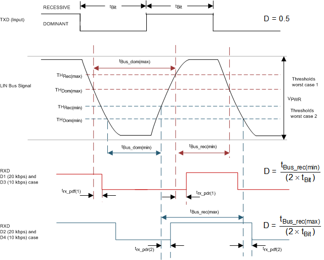 Figure 1. LIN Timing Diagram
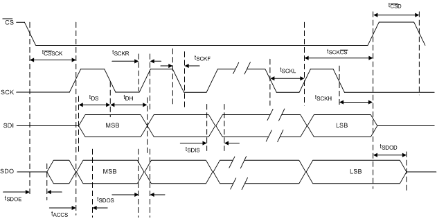 Figure 2. SPI Clocking Details
6.13 Typical Characteristics
VPWR = 12 V, TA = 25°C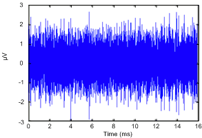
| Input referred LNA AC noise in 10-kHz bandwidth around 40 kHz | ||
| Vnoise = 0.7 µVrms | ||
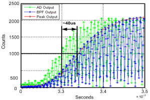
| BPF center frequency = 58 kHz | BPF bandwidth = 7 kHz | |
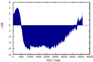
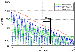
| BPF center frequency = 58 kHz | BPF bandwidth = 7 kHz | |