ZHCSCT4A September 2014 – January 2017 REF1925 , REF1930 , REF1933 , REF1941
PRODUCTION DATA.
8 Parameter Measurement Information
8.1 Solder Heat Shift
The materials used in the manufacture of the REF19xx have differing coefficients of thermal expansion, resulting in stress on the device die when the device is heated. Mechanical and thermal stress on the device die can cause the output voltages to shift, degrading the initial accuracy specifications of the product. Reflow soldering is a common cause of this error.
In order to illustrate this effect, a total of 92 devices were soldered on four printed circuit boards [23 devices on each printed circuit board (PCB)] using lead-free solder paste and the paste manufacturer suggested reflow profile. The reflow profile is as shown in Figure 36. The PCB is comprised of FR4 material. The board thickness is 1.57 mm and the area is 171.54 mm × 165.1 mm.
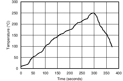 Figure 36. Reflow Profile
The reference and bias output voltages are measured before and after the reflow process; the typical shift is displayed in Figure 37 and Figure 38. Although all tested units exhibit very low shifts (< 0.01%), higher shifts are also possible depending on the size, thickness, and material of the PCB. An important note is that the histograms display the typical shift for exposure to a single reflow profile. Exposure to multiple reflows, which is common on PCBs with surface-mount components on both sides, causes additional shifts in the output bias voltage. If the PCB is exposed to multiple reflows, solder the device in the second pass to minimize device exposure to thermal stress.
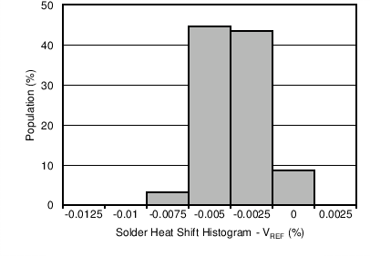 Figure 37. Solder Heat Shift Distribution, VREF (%)
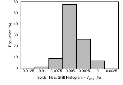 Figure 38. Solder Heat Shift Distribution, VBIAS (%)
8.2 Thermal Hysteresis
Thermal hysteresis is measured with the REF19xx soldered to a PCB, similar to a real-world application. Thermal hysteresis for the device is defined as the change in output voltage after operating the device at 25°C, cycling the device through the specified temperature range, and returning to 25°C. Hysteresis can be expressed by Equation 1:

where
- VHYST = thermal hysteresis (in units of ppm),
- VNOM = the specified output voltage,
- VPRE = output voltage measured at 25°C pre-temperature cycling, and
- VPOST = output voltage measured after the device has cycled from 25°C through the specified temperature range of –40°C to 125°C and returns to 25°C.
Typical thermal hysteresis distribution is as shown in Figure 39 and Figure 40.
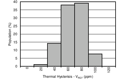 Figure 39. Thermal Hysteresis Distribution (VREF)
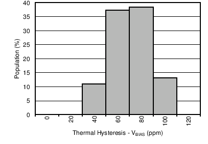 Figure 40. Thermal Hysteresis Distribution (VBIAS)
8.3 Noise Performance
Typical 0.1-Hz to 10-Hz voltage noise is shown in Figure 41 and Figure 42. Device noise increases with output voltage and operating temperature. Additional filtering can be used to improve output noise levels, although care must be taken to ensure the output impedance does not degrade ac performance. Peak-to-peak noise measurement setup is shown in Figure 43.
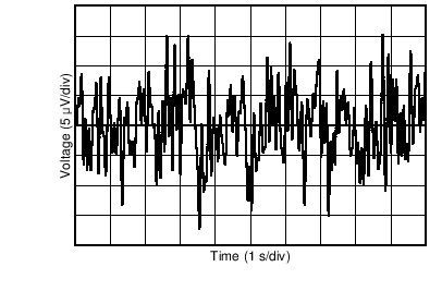 Figure 41. 0.1-Hz to 10-Hz Noise (VREF)
 Figure 42. 0.1-Hz to 10-Hz Noise (VBIAS)
 Figure 43. 0.1-Hz to 10-Hz Noise Measurement Setup