ZHCSCT4A September   2014  – January 2017 REF1925 , REF1930 , REF1933 , REF1941

PRODUCTION DATA.  

  1. 特性
  2. 应用
  3. 说明
  4. 修订历史记录
  5. Device Comparison Table
  6. Pin Configuration and Functions
  7. Specifications
    1. 7.1 Absolute Maximum Ratings
    2. 7.2 ESD Ratings
    3. 7.3 Recommended Operating Conditions
    4. 7.4 Thermal Information
    5. 7.5 Electrical Characteristics
    6. 7.6 Typical Characteristics
  8. Parameter Measurement Information
    1. 8.1 Solder Heat Shift
    2. 8.2 Thermal Hysteresis
    3. 8.3 Noise Performance
  9. Detailed Description
    1. 9.1 Overview
    2. 9.2 Functional Block Diagram
    3. 9.3 Feature Description
      1. 9.3.1 VREF and VBIAS Tracking
      2. 9.3.2 Low Temperature Drift
      3. 9.3.3 Load Current
    4. 9.4 Device Functional Modes
  10. 10Applications and Implementation
    1. 10.1 Application Information
    2. 10.2 Typical Application
      1. 10.2.1 Design Requirements
      2. 10.2.2 Detailed Design Procedure
        1. 10.2.2.1 Shunt Resistor
        2. 10.2.2.2 Differential Amplifier
        3. 10.2.2.3 Voltage Reference
        4. 10.2.2.4 Results
      3. 10.2.3 Application Curves
  11. 11Power-Supply Recommendations
  12. 12Layout
    1. 12.1 Layout Guidelines
    2. 12.2 Layout Example
  13. 13器件和文档支持
    1. 13.1 文档支持
      1. 13.1.1 相关文档 
    2. 13.2 相关链接
    3. 13.3 接收文档更新通知
    4. 13.4 社区资源
    5. 13.5 商标
    6. 13.6 静电放电警告
    7. 13.7 Glossary
  14. 14机械、封装和可订购信息

封装选项

机械数据 (封装 | 引脚)
散热焊盘机械数据 (封装 | 引脚)
订购信息

Power-Supply Recommendations

The REF19xx family of references feature an extremely low-dropout voltage. These references can be operated with a supply of only 20 mV above the output voltage. For loaded reference conditions, a typical dropout voltage versus load is shown in Figure 53. A supply bypass capacitor ranging between 0.1 µF to 10 µF is recommended.
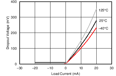
REF1925 REF1930 REF1933 REF1941 C005_SBOS600.png Figure 53. Dropout Voltage vs Load Current