ZHCSGP1 September   2017 REF2125

PRODUCTION DATA.  

  1. 特性
  2. 应用
  3. 说明
  4. 修订历史记录
  5. Pin Configuration and Functions
  6. Specifications
    1. 6.1 Absolute Maximum Ratings
    2. 6.2 ESD Ratings
    3. 6.3 Recommended Operating Conditions
    4. 6.4 Thermal Information
    5. 6.5 Electrical Characteristics
    6. 6.6 Typical Characteristics
  7. Parameter Measurement Information
    1. 7.1 Solder Heat Shift
    2. 7.2 Long-Term Stability
    3. 7.3 Thermal Hysteresis
    4. 7.4 Power Dissipation
    5. 7.5 Noise Performance
  8. Detailed Description
    1. 8.1 Overview
    2. 8.2 Functional Block Diagram
    3. 8.3 Feature Description
      1. 8.3.1 Supply Voltage
      2. 8.3.2 Low Temperature Drift
      3. 8.3.3 Load Current
      4. 8.3.4 Clean Start Feature
    4. 8.4 Device Functional Modes
      1. 8.4.1 EN Pin
      2. 8.4.2 Negative Reference Voltage
  9. Applications and Implementation
    1. 9.1 Application Information
    2. 9.2 Typical Application: Basic Voltage Reference Connection
      1. 9.2.1 Design Requirements
      2. 9.2.2 Detailed Design Procedure
        1. 9.2.2.1 Input and Output Capacitors
        2. 9.2.2.2 VIN Slew Rate Considerations
        3. 9.2.2.3 Shutdown/Enable Feature
      3. 9.2.3 Application Curves
  10. 10Power-Supply Recommendations
  11. 11Layout
    1. 11.1 Layout Guidelines
    2. 11.2 Layout Example
  12. 12器件和文档支持
    1. 12.1 文档支持
      1. 12.1.1 相关文档
    2. 12.2 接收文档更新通知
    3. 12.3 社区资源
    4. 12.4 商标
    5. 12.5 静电放电警告
    6. 12.6 Glossary
  13. 13机械、封装和可订购信息

封装选项

机械数据 (封装 | 引脚)
散热焊盘机械数据 (封装 | 引脚)
订购信息

Layout

Layout Guidelines

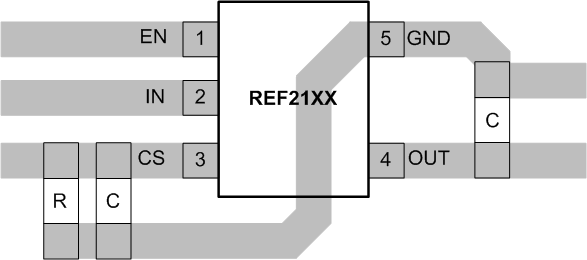
Figure 31 illustrates an example of a PCB layout for a data acquisition system using the REF2125. Some key considerations are:

  • Connect low-ESR, 0.1-μF ceramic bypass capacitors at VIN, VREF of the REF2125.
  • Decouple other active devices in the system per the device specifications.
  • Using a solid ground plane helps distribute heat and reduces electromagnetic interference (EMI) noise pickup.
  • Place the external components as close to the device as possible. This configuration prevents parasitic errors (such as the Seebeck effect) from occurring.
  • Do not run sensitive analog traces in parallel with digital traces. Avoid crossing digital and analog traces if possible, and only make perpendicular crossings when absolutely necessary.

Layout Example

REF2125 layout_SBAS798.gif Figure 31. Layout Example