ZHCSGP1 September 2017 REF2125
PRODUCTION DATA.
6 Specifications
6.1 Absolute Maximum Ratings
over operating free-air temperature range (unless otherwise noted)(1)| MIN | MAX | UNIT | ||
|---|---|---|---|---|
| Input voltage | IN | VREF + 0.05 | 13 | V |
| EN | –0.3 | IN + 0.3 | ||
| Output voltage | VREF | –0.3 | 5.5 | V |
| Output short circuit current | 20 | mA | ||
| Temperature | Operating, TA | –55 | 150 | °C |
| Storage Tstg | –65 | 170 | ||
(1) Stresses beyond those listed under Absolute Maximum Ratings may cause permanent damage to the device. These are stress ratings only, which do not imply functional operation of the device at these or any other conditions beyond those indicated under Recommended Operating Conditions. Exposure to absolute-maximum-rated conditions for extended periods may affect device reliability.
6.2 ESD Ratings
| VALUE | UNIT | |||
|---|---|---|---|---|
| V(ESD) | Electrostatic discharge | Human-body model (HBM), per ANSI/ESDA/JEDEC JS-001(1) | ±1000 | V |
| Charged-device model (CDM), per JEDEC specification JESD22-C101(2) | ±250 | |||
(1) JEDEC document JEP155 states that 500-V HBM allows safe manufacturing with a standard ESD control process.
(2) JEDEC document JEP157 states that 250-V CDM allows safe manufacturing with a standard ESD control process.
6.3 Recommended Operating Conditions
over operating free-air temperature range (unless otherwise noted)| MIN | NOM | MAX | UNIT | ||
|---|---|---|---|---|---|
| IN | Supply input voltage (IL = 0 mA, TA = 25°C) | VREF + VDO (1) | 12 | V | |
| EN | Enable voltage | 0 | IN | V | |
| IL | Output current | –10 | 10 | mA | |
| TA | Operating temperature | –40 | 25 | 125 | °C |
(1) Dropout voltage.
6.4 Thermal Information
| THERMAL METRIC(1) | REF2125 | UNIT | |
|---|---|---|---|
| DBV (SOT-23) | |||
| 6 PINS | |||
| RθJA | Junction-to-ambient thermal resistance | 185 | °C/W |
| RθJC(top) | Junction-to-case (top) thermal resistance | 156 | °C/W |
| RθJB | Junction-to-board thermal resistance | 29.6 | °C/W |
| ψJT | Junction-to-top characterization parameter | 33.8 | °C/W |
| ψJB | Junction-to-board characterization parameter | 29.1 | °C/W |
| RθJC(bot) | Junction-to-case (bottom) thermal resistance | N/A | °C/W |
(1) For more information about traditional and new thermal metrics, see the Semiconductor and IC Package Thermal Metrics application report.
6.5 Electrical Characteristics
At TA = 25°C unless otherwise noted.| PARAMETER | TEST CONDITIONS | MIN | TYP | MAX | UNIT | ||
|---|---|---|---|---|---|---|---|
| ACCURACY AND DRIFT | |||||||
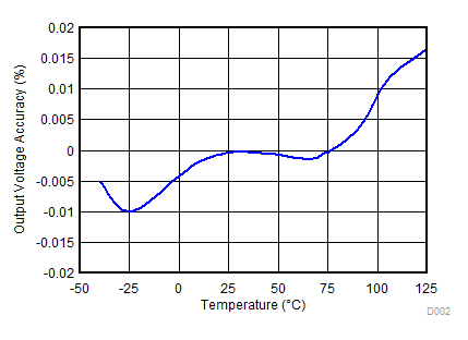
| Output voltage accuracy | –40°C ≤ TA ≤ 125°C | –0.05% | 0.05% | ||||
| Output voltage temperature coefficient(1) | 2.5 | 6 | ppm/°C | ||||
| LINE AND LOAD REGULATION | |||||||
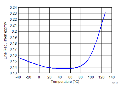
| ΔV(OΔVIN) | Line regulation | VIN = 2.55 V to 12 V , TA = 25°C | 2 | ppm/V | |||
| VIN = VREF + VDO(5) to 12 V, −40°C ≤ TA ≤ 125°C | 15 | ||||||
| ΔV(OΔIL) | Load regulation | IL = 0 mA to 10 mA, VIN = 3 V, TA = 25°C | Sourcing | 20 | ppm/mA | ||
| IL = 0 mA to 10 mA, VIN = 3 V, −40°C ≤ TA ≤ 125°C | Sourcing | 30 | |||||
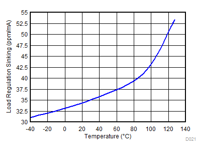
| IL = 0 mA to –10 mA, VIN = VREF+ VDO(5), TA = 25°C | Sinking | 40 | |||||
| IL = 0 mA to –10 mA, VIN = VREF+ VDO(5), −40°C ≤ TA ≤ 125°C | Sinking | 70 | |||||
| ISC | Short-circuit current(6) | VREF = 0, CCS = No connect, TA = 25°C | 18 | mA | |||
| RCS = 500kΩ, TA = 25°C | 7 | mA | |||||
| CCS = GND, TA = 25°C | 0.5 | mA | |||||
| NOISE | |||||||
| en p-p | Output voltage noise(2) | ƒ = 0.1 Hz to 10 Hz | 5 | μV p-p/V | |||
| ƒ = 10 Hz to 10 kHz | 24 | μV rms | |||||
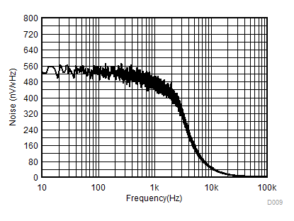
| en | Output voltage noise density | ƒ = 1 kHz | 0.25 | ppm/√Hz | |||
| HYSTERESIS AND LONG TERM STABILITY | |||||||
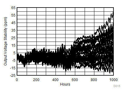
| Long-term stability(3) | 1000 hours | 30 | ppm | ||||
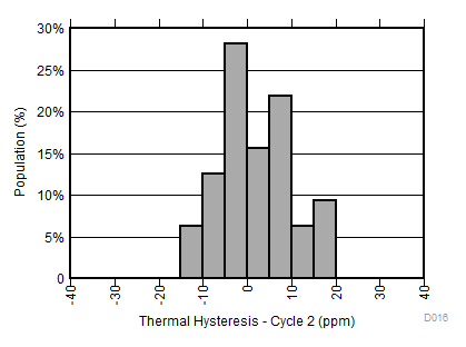
| Output voltage hysteresis(4) | TA = 25°C to −40°C to 125°C to 25°C, Cycle 1 | 30 | ppm | ||||
| TA = 25°C to −40°C to 125°C to 25°C, Cycle 2 | 10 | ||||||
| TURNON | |||||||
| tON | Turnon time | 0.1% of output voltage settling, CL = 10 µF, REF2125 | 2.5 | ms | |||
| CAPACITIVE LOAD | |||||||
| CL | Stable output capacitor value | −40°C ≤ TA ≤ 125°C | 0.1 | 10 | µF | ||
| OUTPUT VOLTAGE | |||||||
| VREF | Output voltage | REF2125 | 2.5 | V | |||
| POWER SUPPLY | |||||||
| VIN | Input voltage | VREF + VDO | 12 | V | |||
| IL | Output current capacity | VIN = VREF + VDO(5) to 12 V | Sourcing | 10 | mA | ||
| VIN = VREF + VDO(5) to 12 V | Sinking | –10 | |||||
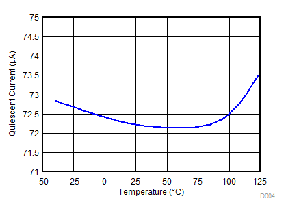
| IQ | Quiescent current | −40°C ≤ TA ≤ 125°C | Active mode | 72 | 95 | µA | |
| −40°C ≤ TA ≤ 125°C | Shutdown mode | 2.5 | 3 | ||||
| VDO | Dropout voltage | IL = 0 mA, TA= 25°C | 50 | mV | |||
| IL = 0 mA, −40°C ≤ TA ≤ +125°C | 100 | ||||||
| IL = 10 mA, −40°C ≤ TA ≤ +125°C | 500 | ||||||
| VEN | ENABLE pin voltage | Voltage reference in active mode (EN = 1) | 1.6 | V | |||
| Voltage reference in shutdown mode (EN = 0) | 0.5 | ||||||
| IEN | ENABLE pin leakage current | ENABLE = VIN, −40°C ≤ TA ≤ 125°C | 1 | 2 | µA | ||
(1) Temperature drift is specified according to the box method. See Feature Description for more details.
(2) The peak-to-peak noise measurement procedure is explained in more detail in Noise Performance.
(3) Long-term stability measurement procedure is explained in more in detail in Long-Term Stability.
(4) The thermal hysteresis measurement procedure is explained in more detail in Thermal Hysteresis.
(5) Dropout voltage under test condition is 100mV.
(6) In clean start section it is referred as IPEAK.
6.6 Typical Characteristics
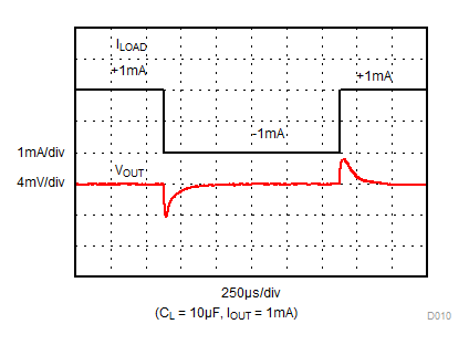
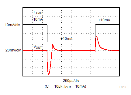
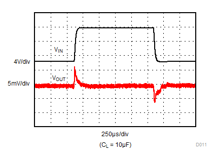
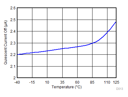
at TA = 25°C, VIN = VEN = 12 V, IL = 0 mA , CL = 10 µF, CIN = 0.1 µF (unless otherwise noted)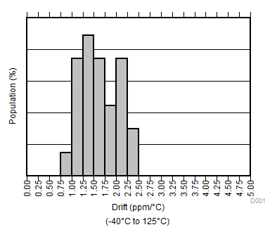
1.
Figure 19. Load Regulation Sinking
1.
Figure 21. Long Term Stability - 1000 hours (VREF)
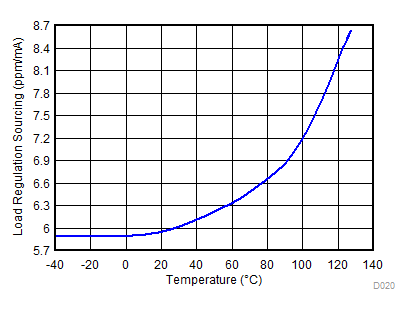
1.
Figure 18. Load Regulation Sourcing
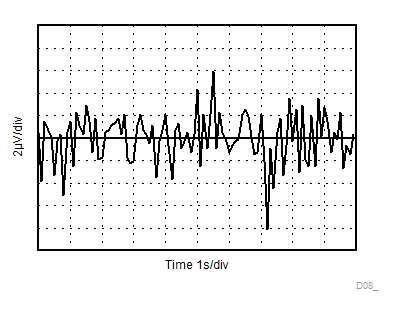
1.
Figure 20. 0.1-Hz to 10-Hz Noise (VREF)
