ZHCSGP1 September 2017 REF2125
PRODUCTION DATA.
8 Detailed Description
8.1 Overview
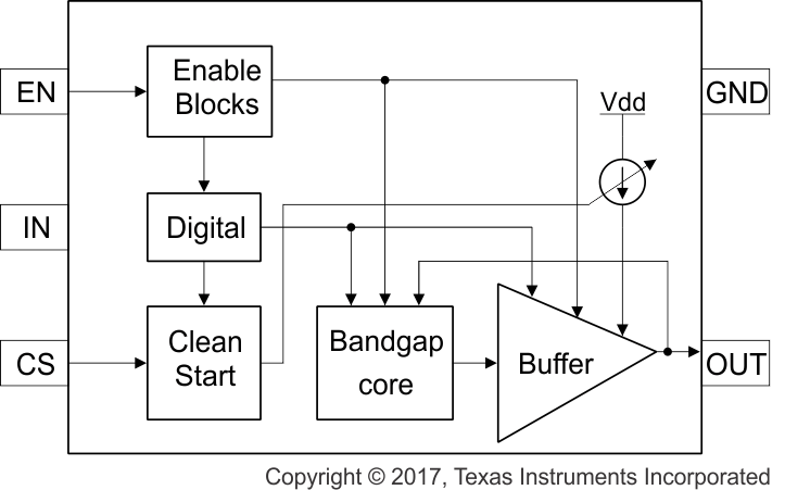
The REF2125 is part of a family of low-noise, precision bandgap voltage references that are specifically designed for excellent initial voltage accuracy and drift. The Functional Block Diagram is a simplified block diagram of the REF2125 showing basic band-gap topology.
8.2 Functional Block Diagram

8.3 Feature Description
8.3.1 Supply Voltage
The REF2125 family of references features an extremely low dropout voltage. The REF2125 can be operated with a supply of only 1 mV above the output voltage in an unloaded condition. For loaded conditions, a typical dropout voltage versus load is shown on the front page. The REF2125 features a low quiescent current that is extremely stable over changes in both temperature and supply. The typical room temperature quiescent current is 72 μA, and the maximum quiescent current over temperature is just 95 μA. Supply voltages below the specified levels can cause the REF2125 to momentarily draw currents greater than the typical quiescent current. Use a power supply with a fast rising edge and low output impedance to easily prevent this issue.
8.3.2 Low Temperature Drift
The REF2125 is designed for minimal drift error, which is defined as the change in output voltage over temperature. The drift is calculated using the box method, as described by Equation 3:

8.3.3 Load Current
The REF2125 family is specified to deliver a current load of ±10 mA per output. The VREF output of the device are protected from short circuits by limiting the output short-circuit current to 18 mA. The device temperature increases according to Equation 4:

where
- TJ = junction temperature (°C),
- TA = ambient temperature (°C),
- PD = power dissipated (W), and
- RθJA = junction-to-ambient thermal resistance (°C/W)
The REF2125 maximum junction temperature must not exceed the absolute maximum rating of 150°C.
8.3.4 Clean Start Feature
In many applications (for example, loop powered applications), the supply at VIN has inductive impedance. This can cause the supply to dip during start-up because of the large output capacitor connected to the voltage reference and the inductive supply. The REF2125 family has an internal clean start block to control the peak of the inrush current during start-up. This feature is illustrated in Functional Block Diagram. The peak of inrush current can be calculated as Equation 5:

where
- IPEAK = Peak of inrush current (µA), has a range of [0.5 mA, 19 mA],
- Rcs = External resistor connected to the CS pin
During power up, IPEAK is split between the device current and output current. The output current (IOUT) is split between output capacitor and load current (ILOAD). The device current can be estimated to be IQ+IOUT/183, where IQ is quiescent current at no load. Hence for a given ILOAD it is important to choose Rcs such that IPEAK is larger than ILOAD. Above equations capture typical characteristics and hence it is suggested to include ±25% margins while budgeting for inrush current and also while choosing Rcs for a given ILOAD. This inrush current continues to stay at the limiting value (IPEAK) till output reaches close to VREF (2.5 V).
When a Ccs is also connected in parallel to Rcs, The inrush current limit shall rise exponentially to the steady state value (IPEAK) as calculated using above equations, with a time constant of Rcs × Ccs. Hence the initial (and maximum) rate of rise of inrush current shall be IPEAK /(Rcs × Ccs). Because the inrush current rate is limited, the loop powered supply dip is controlled.
8.4 Device Functional Modes
8.4.1 EN Pin
When the ENABLE pin of the REF2125 is pulled high, the device is in active mode. The device must be in active mode for normal operation. The REF2125 can be placed in a low-power mode by pulling the ENABLE pin low. When in shutdown mode, the output of the device becomes high impedance and the quiescent current of the device reduces to 2 µA in shutdown mode. The EN pin must not be pulled higher than VIN supply voltage. See the Thermal Information for logic high and logic low voltage levels.
8.4.2 Negative Reference Voltage
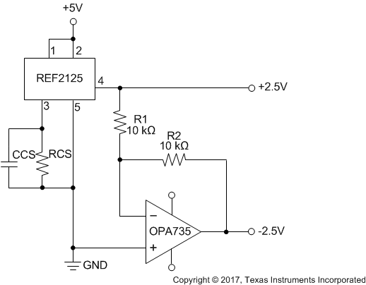
For applications requiring a negative and positive reference voltage, the REF2125 and OPA735 can be used to provide a dual-supply reference from a 5-V supply. Figure 27 shows the REF2125 used to provide a 2.5-V supply reference voltage. The low drift performance of the REF2125 complements the low offset voltage and zero drift of the OPA735 to provide an accurate solution for split-supply applications. Take care to match the temperature coefficients of R1 and R2.
 Figure 27. REF2125 and OPA735 Create Positive and Negative Reference Voltages