SBOS392H August   2007  – August 2019 REF3312 , REF3318 , REF3320 , REF3325 , REF3330 , REF3333

PRODUCTION DATA.  

  1. Features
  2. Applications
  3. Description
    1.     Device Images
      1.      REF3312 in a Single-Supply Signal Chain
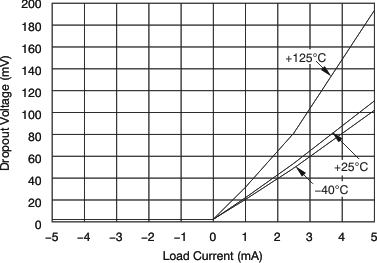
      2.      Dropout Voltage vs Load Current
  4. Revision History
  5. Device Comparison
  6. Pin Configuration and Functions
    1. Table 1. Pin Functions
  7. Specifications
    1. 7.1 Absolute Maximum Ratings
    2. 7.2 ESD Ratings
    3. 7.3 Recommended Operating Conditions
    4. 7.4 Thermal Information
    5. 7.5 Electrical Characteristics
    6. 7.6 Typical Characteristics
  8. Parameter Measurement Information
    1. 8.1 Thermal Hysteresis
  9. Detailed Description
    1. 9.1 Overview
    2. 9.2 Functional Block Diagram
    3. 9.3 Feature Description
      1. 9.3.1 Start-Up Time
      2. 9.3.2 Low Temperature Drift
      3. 9.3.3 Power Dissipation
      4. 9.3.4 Noise Performance
    4. 9.4 Device Functional Modes
  10. 10Applications and Implementation
    1. 10.1 Application Information
    2. 10.2 Typical Applications
      1. 10.2.1 REF3312 in a Bipolar Signal-Chain Configuration
        1. 10.2.1.1 Design Requirements
        2. 10.2.1.2 Detailed Design Procedure
          1. 10.2.1.2.1 Op Amp Level-Shift Design
          2. 10.2.1.2.2 Differential Input Attenuator Design
          3. 10.2.1.2.3 Input Filtering
          4. 10.2.1.2.4 Component Selection
            1. 10.2.1.2.4.1 Voltage References
            2. 10.2.1.2.4.2 Op Amp
          5. 10.2.1.2.5 Input Attenuation and Level Shifting
          6. 10.2.1.2.6 Input Filtering
          7. 10.2.1.2.7 Passive Component Tolerances and Materials
        3. 10.2.1.3 Application Curves
          1. 10.2.1.3.1 DC Performance
          2. 10.2.1.3.2 AC Performance
  11. 11Power-Supply Recommendations
  12. 12Layout
    1. 12.1 Layout Guidelines
    2. 12.2 Layout Example
  13. 13Device and Documentation Support
    1. 13.1 Documentation Support
      1. 13.1.1 Related Documentation
    2. 13.2 Related Links
    3. 13.3 Receiving Notification of Documentation Updates
    4. 13.4 Community Resources
    5. 13.5 Trademarks
    6. 13.6 Electrostatic Discharge Caution
    7. 13.7 Glossary
  14. 14Mechanical, Packaging, and Orderable Information

封装选项

机械数据 (封装 | 引脚)
散热焊盘机械数据 (封装 | 引脚)
订购信息

Typical Characteristics

At TA = 25°C and VIN = 5 V, and REF3325 used for typical characteristic measurements (unless otherwise noted).
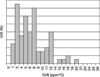
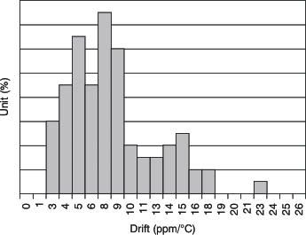
REF3312 REF3318 REF3320 REF3325 REF3330 REF3333 tc_tmp_drift_70c_bos392.gif
0°C to 70°C
Figure 1. Temperature Drift
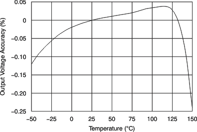
REF3312 REF3318 REF3320 REF3325 REF3330 REF3333 tc_vo_acc-tmp_bos392.gif
Figure 3. Output Voltage Accuracy vs Temperature
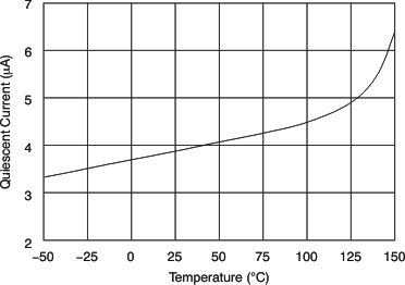
REF3312 REF3318 REF3320 REF3325 REF3330 REF3333 tc_iq-tmp_bos392.gif
Figure 5. Quiescent Current vs Temperature
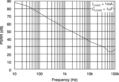
REF3312 REF3318 REF3320 REF3325 REF3330 REF3333 tc_psrr_bos392.gif
Figure 7. Power-Supply Rejection Ratio vs Frequency
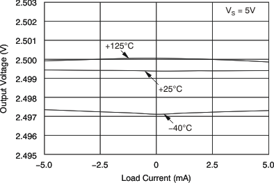
REF3312 REF3318 REF3320 REF3325 REF3330 REF3333 tc_vo-iload_bos392.gif
Figure 9. Output Voltage vs Load Current
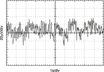
REF3312 REF3318 REF3320 REF3325 REF3330 REF3333 tc_noise_bos392.gif
Figure 11. 0.1-Hz to 10-Hz Noise
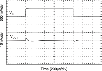
REF3312 REF3318 REF3320 REF3325 REF3330 REF3333 tc_line_trans_0ma_bos392.gif
CLOAD = 10 μF, IOUT = 0 mA
Figure 13. Line Transient
REF3312 REF3318 REF3320 REF3325 REF3330 REF3333 tc_line_trans_1ma_bos392.gif
CLOAD = 10 μF, IOUT = 1 mA
Figure 15. Line Transient
REF3312 REF3318 REF3320 REF3325 REF3330 REF3333 tc_tmp_drift_125c_bos392.gif
–40°C to 125°C
Figure 2. Temperature Drift
REF3312 REF3318 REF3320 REF3325 REF3330 REF3333 tc_vdo-iload_bos392.gif
Figure 4. Dropout Voltage vs Load Current
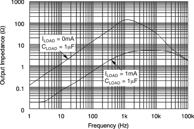
REF3312 REF3318 REF3320 REF3325 REF3330 REF3333 tc_io-frq_bos392.gif
Figure 6. Output Impedance vs Frequency
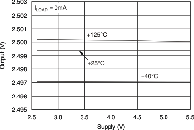
REF3312 REF3318 REF3320 REF3325 REF3330 REF3333 tc_out-sup_bos392.gif
Figure 8. Output vs Supply
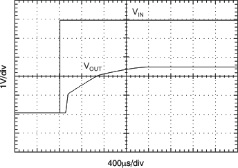
REF3312 REF3318 REF3320 REF3325 REF3330 REF3333 tc_step_1uf_bos392.gif
CL = 1-μF Startup
Figure 10. Step Response
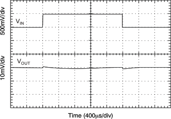
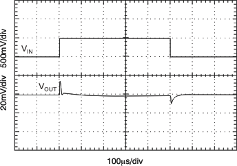
REF3312 REF3318 REF3320 REF3325 REF3330 REF3333 tc_line_trans_bos392.gif
CL = 1 μF, IOUT = 0 mA
Figure 12. Line Transient
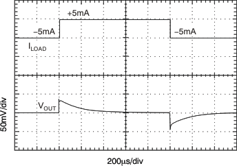
REF3312 REF3318 REF3320 REF3325 REF3330 REF3333 tc_load_trans_5ma_bos392.gif
CL = 1 μF, ±5-mA Output Pulse
Figure 14. Load Transient
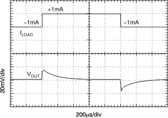
REF3312 REF3318 REF3320 REF3325 REF3330 REF3333 tc_load_trans_1ma_bos392.gif
CL = 1 μF, ±1-mA Output Pulse
Figure 16. Load Transient