ZHCSGP2F September 2017 – June 2021 REF3425 , REF3430 , REF3433 , REF3440 , REF3450
PRODUCTION DATA
- 1 特性
- 2 应用
- 3 说明
- 4 Revision History
- 5 Device Comparison Table
- 6 Pin Configuration and Functions
- 7 Specifications
- 8 Parameter Measurement Information
- 9 Detailed Description
- 10Application and Implementation
- 11Power Supply Recommendations
- 12Layout
- 13Device and Documentation Support
- 14Mechanical, Packaging, and Orderable Information
6 Pin Configuration and Functions
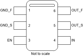
 Figure 6-1 REF34xx
DBV Package
6-Pin SOT-23
Top View
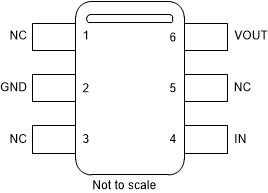
 Figure 6-2 REF34xxT
DBV Package
6-Pin SOT-23
Top View
Table 6-1 Pin Functions
| PIN | TYPE | DESCRIPTION | ||
|---|---|---|---|---|
| NAME | REF34xx (DBV) | REF34xxT (DBV) | ||
| GND_F | 1 | Ground | Ground force connection. | |
| GND_S | 2 | Ground | Ground sense connection. | |
| GND | 2 | Ground | Device ground. | |
| EN | 3 | Input | Enable connection. Enables or disables the device. | |
| IN | 4 | 4 | Power | Input supply voltage connection. |
| OUT_S | 5 |
Input |
Reference voltage output sense connection. | |
| OUT_F | 6 | Output | Reference voltage output force connection. | |
| VOUT | 6 | Output | Reference voltage output connection. | |
| NC | 1,3,5 | - | Not connected. Pin can be left floating or connected to voltage within device operating range. | |