SBOS471B April   2010  – June 2015 REF5020-EP , REF5025-EP , REF5040-EP , REF5050-EP

PRODUCTION DATA.  

  1. Features
  2. Applications
  3. Description
  4. Revision History
  5. Pin Configuration and Functions
  6. Specifications
    1. 6.1 Absolute Maximum Ratings
    2. 6.2 ESD Ratings
    3. 6.3 Recommended Operating Conditions
    4. 6.4 Thermal Information
    5. 6.5 Electrical Characteristics: Per Device
    6. 6.6 Electrical Characteristics: All Devices
    7. 6.7 Typical Characteristics
  7. Detailed Description
    1. 7.1 Overview
    2. 7.2 Functional Block Diagram
    3. 7.3 Feature Description
      1. 7.3.1 Output Adjustment Using The TRIM/NR Pin
      2. 7.3.2 Low Temperature Drift
      3. 7.3.3 Temperature Monitoring
      4. 7.3.4 Noise Performance
    4. 7.4 Device Functional Modes
  8. Application and Implementation
    1. 8.1 Application Information
    2. 8.2 Typical Applications
      1. 8.2.1 Negative Reference Voltage
        1. 8.2.1.1 Design Requirements
        2. 8.2.1.2 Detailed Design Procedure
        3. 8.2.1.3 Application Curves
      2. 8.2.2 Positive Reference Voltage
        1. 8.2.2.1 Detailed Design Procedure
          1. 8.2.2.1.1 Load Capacitance
          2. 8.2.2.1.2 Bandgap Noise Reduction
    3. 8.3 System Example
      1. 8.3.1 Data Acquisition
  9. Power Supply Recommendations
    1. 9.1 Basic Connections
    2. 9.2 Low Dropout Voltage
  10. 10Layout
    1. 10.1 Layout Guidelines
    2. 10.2 Layout Example
    3. 10.3 Power Dissipation
  11. 11Device and Documentation Support
    1. 11.1 Documentation Support
      1. 11.1.1 Related Documentation
    2. 11.2 Related Links
    3. 11.3 Community Resources
    4. 11.4 Trademarks
    5. 11.5 Electrostatic Discharge Caution
    6. 11.6 Glossary
  12. 12Mechanical, Packaging, and Orderable Information

封装选项

机械数据 (封装 | 引脚)
散热焊盘机械数据 (封装 | 引脚)
订购信息

5 Pin Configuration and Functions

D Package
8- Pin SOIC
Top View
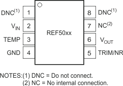
REF5020-EP REF5025-EP REF5040-EP REF5050-EP pin_diagram_bos471.gif

Pin Functions

PIN I/O DESCRIPTION
NAME NO.
DNC 1 Do not connect
VIN 2 Power Power supply voltage. Range from VOUT + 0.2 V up to 18 V. Recommended bypass capacitor from 1 µF up to 10 µF
TEMP 3 O Temperature monitoring pin provides a temperature-dependent voltage output
GND 4 Power System ground
TRIM/NR 5 I Output adjustment and noise reduction input. Connecting 1 µF to this pin will create low pas filter at the bandgap and reduce output noise
VOUT 6 O Very accurate, factory-trimmed voltage output. Recommended bypass capacitor from 1 µF up to 50 µF with ESR between 1 and 1.5 Ω
NC 7 No internal connection
DNC 8 Do not connect