SBOS502F September 2009 – December 2016 REF5025-HT
PRODUCTION DATA.
- 1 Features
- 2 Applications
- 3 Description
- 4 Revision History
- 5 Pin Configuration and Functions
- 6 Specifications
- 7 Detailed Description
- 8 Application and Implementation
- 9 Power Supply Recommendations
- 10Layout
- 11Device and Documentation Support
- 12Mechanical, Packaging, and Orderable Information
封装选项
机械数据 (封装 | 引脚)
散热焊盘机械数据 (封装 | 引脚)
订购信息
5 Pin Configuration and Functions
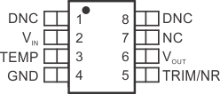
HKJ Package
8-Pin CFP
Top View

DNC = Do not connect
NC = No internal connection
NC = No internal connection
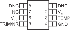
HKQ Package
8-Pin CFP
Top View

HKQ is a dead bug performed version of HKJ
Pin Functions
| PIN | I/O | DESCRIPTION | |
|---|---|---|---|
| NAME | NO. | ||
| DNC | 1, 8 | — | Do not connect |
| GND | 4 | Power | System ground |
| NC | 7 | — | No internal connection |
| TEMP | 3 | O | Temperature monitoring pin provides a temperature-dependent voltage output |
| TRIM/NR | 5 | I | Output adjustment and noise reduction input. Connecting 1 μF to this pin creates a low-pass filter at the bandgap and reduce output noise |
| VIN | 2 | Power | Power supply voltage. Range from VOUT + 0.2 V up to 18 V. TI recommends a bypass capacitor with a value from 1 μF up to 10 μF |
| VOUT | 6 | O | Very accurate, factory-trimmed voltage output. TI recommends a bypass capacitor with a value from 1 μF up to 50 μF with ESR between 1 and 1.5 Ω |
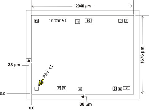
Bare Die Information
| DIE THICKNESS | BACKSIDE FINISH | BACKSIDE POTENTIAL | BOND PAD METALLIZATION COMPOSITION | BOND PAD THICKNESS |
|---|---|---|---|---|
| 15 mils | Silicon with backgrind | GND | Al-Cu (0.5%) | 598 nm |

Bond Pad Coordinates in Microns
| DESCRIPTION | PAD NUMBER | X MIN | Y MIN | X MAX | Y MAX |
|---|---|---|---|---|---|
| NC | 1 | 35.45 | 46.55 | 111.45 | 122.55 |
| NC | 2 | 496.75 | 56.55 | 572.75 | 132.55 |
| VIN | 3 | 607.45 | 56.55 | 683.45 | 132.55 |
| NC | 4 | 637.9 | 39.4 | 1013.9 | 115.4 |
| TEMP | 5 | 1660.1 | 47.2 | 1736.1 | 123.2 |
| GND | 6 | 1770.9 | 38.85 | 1847.05 | 115 |
| GND | 7 | 1877.1 | 59.6 | 2016.8 | 135.6 |
| TRIM/NR | 8 | 1904.65 | 1553.4 | 1980.65 | 1629.4 |
| NC | 9 | 1782.15 | 1553.4 | 1858.15 | 1629.4 |
| VOUT | 10 | 1080.2 | 1559.85 | 1219.9 | 1636 |
| VOUT | 11 | 880.25 | 1543.55 | 956.25 | 1619.55 |
| NC | 12 | 35.45 | 1553.45 | 111.45 | 1629.45 |