6 Specifications
6.1 Absolute Maximum Ratings
over operating free-air temperature range (unless otherwise noted)(1)
|
MIN |
MAX |
UNIT |
| Input voltage |
VIN |
|
18 |
V |
| Output short-circuit |
|
30 |
mA |
| Operating temperature |
–55 |
210 |
°C |
| Junction temperature, TJ |
|
210 |
°C |
| Storage temperature, Tstg |
–65 |
210 |
°C |
(1) Stresses beyond those listed under Absolute Maximum Ratings may cause permanent damage to the device. These are stress ratings only, which do not imply functional operation of the device at these or any other conditions beyond those indicated under Recommended Operating Conditions. Exposure to absolute-maximum-rated conditions for extended periods may affect device reliability.
6.2 ESD Ratings
|
VALUE |
UNIT |
| V(ESD) |
Electrostatic discharge |
Human body model (HBM), per ANSI/ESDA/JEDEC JS-001(1) |
±3000 |
V |
| Charged-device model (CDM), per JEDEC specification JESD22-C101(2) |
±1000 |
(1) JEDEC document JEP155 states that 500-V HBM allows safe manufacturing with a standard ESD control process.
(2) JEDEC document JEP157 states that 250-V CDM allows safe manufacturing with a standard ESD control process.
6.3 Recommended Operating Conditions
over operating free-air temperature range (unless otherwise noted)
|
MIN |
MAX |
UNIT |
| VIN |
3.25 |
18 |
V |
| IOUT |
–7 |
7 |
mA |
6.4 Thermal Information
| THERMAL METRIC(1) |
REF5025-HT |
UNIT |
| HJK, HKQ (CFP) |
| 8 PINS |
| RθJC |
Junction-to-case thermal resistance |
To ceramic side of case |
5.7 |
°C/W |
| To top of case lid (metal side of case) |
13.7 |
6.5 Electrical Characteristics
at TA = 25°C, ILOAD = 0, CL = 1 μF, VIN = 3.25 V to 18 V (unless otherwise noted).
| PARAMETER |
TEST CONDITIONS |
TA = –55 to +125°C |
TA = 210°C |
UNIT |
| MIN |
TYP |
MAX |
MIN |
TYP |
MAX |
| OUTPUT VOLTAGE (2.5 V) |
| VOUT |
Output voltage |
|
|
2.5 |
|
|
2.5 |
|
V |
|
Initial accuracy(1) |
VIN = 3.25 V |
0% |
|
0.9% |
|
0.14% |
|
|
| NOISE |
|
Output voltage noise |
f = 0.1 Hz to 10 Hz |
|
7.5 |
|
|
|
|
μVPP |
| OUTPUT VOLTAGE TEMPERATURE DRIFT |
| dVOUT/dT |
Output voltage temperature drift(2) |
Calculated from
–55°C to +210°C |
|
|
|
|
|
40 |
ppm/°C |
| LINE REGULATION |
| dVOUT/dVIN |
Line regulation |
From VIN = 3.25 V to VIN = 18 V |
|
1 |
2.2 |
|
63 |
215 |
ppm/V |
| LOAD REGULATION |
| dVOUT/dILOAD |
Load regulation |
–7 mA < ILOAD < 10 mA, VIN = 3.25 V |
|
20 |
50 |
|
20 |
75 |
ppm/mA |
| SHORT-CIRCUIT CURRENT |
| ISC |
Short-circuit current |
VOUT = 0 V |
|
25 |
|
|
11 |
|
mA |
| TEMP PIN |
|
Voltage output |
At TA = 25°C |
|
575 |
|
|
|
|
mV |
| Temperature sensitivity(3) |
|
|
2.64 |
|
|
|
|
mV/°C |
| TURN-ON SETTLING TIME |
|
Turn-on settling time |
To 0.1% with CL = 1 μF |
|
200 |
|
|
|
|
μs |
| POWER SUPPLY |
|
|
|
|
|
|
|
|
| VS |
Supply voltage |
|
3.25 |
|
18 |
3.25 |
|
18 |
V |
|
Quiescent current |
|
|
0.8 |
1.2 |
|
|
1.5 |
mA |
| TEMPERATURE RANGE |
|
Specified range |
–55°C to +210°C |
|
|
|
|
|
|
|
|
Operating range |
–55°C to +210°C |
|
|
|
|
|
|
|
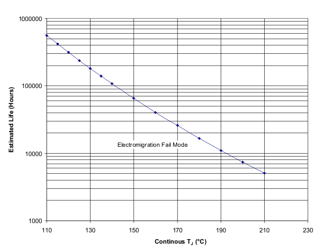
2. Silicon operating life design goal is 10 years at 105°C junction temperature (does not include package interconnect life).
Figure 1. REF5025SKGD1 and REF5025SKGD2 Operating Life Derating Chart
6.6 Typical Characteristics
at TA = 25°C, ILOAD = 0, VS = 3.25 V (unless otherwise noted).
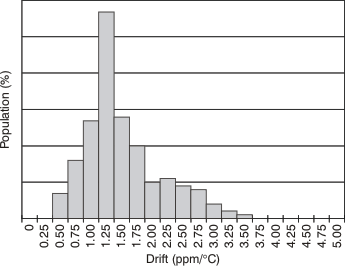 Figure 2. Temperature Drift (0°C to 85°C)
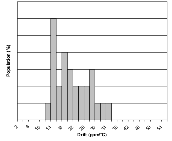 Figure 4. Temperature Drift (–55°C to +210°C)
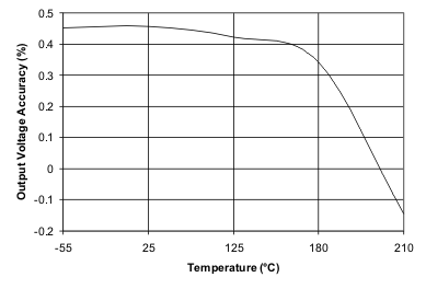 Figure 6. Output Voltage Accuracy vs Temperature
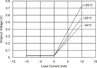 Figure 8. Dropout Voltage vs Load Current
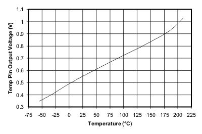 Figure 10. Temperature Pin Output Voltage vs Temperature
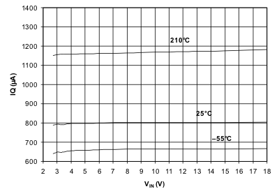 Figure 12. Quiescent Current vs Input Voltage
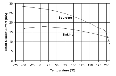 Figure 14. Short-Circuit Current vs Temperature
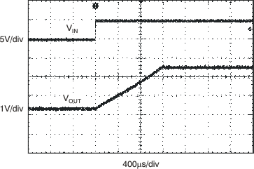
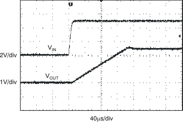 Figure 16. Start-Up (REF5025)
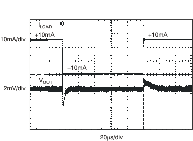
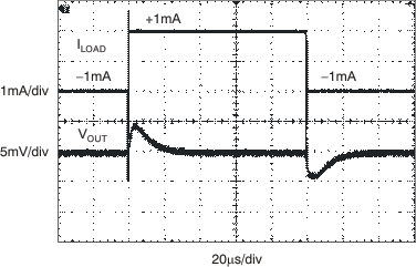 Figure 18. Load Transient
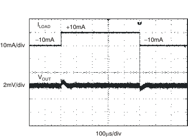
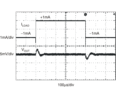 Figure 20. Load Transient
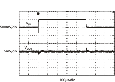
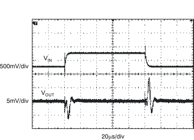 Figure 22. Line Transient
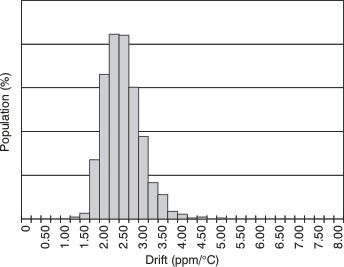 Figure 3. Temperature Drift (–40°C to +125°C)
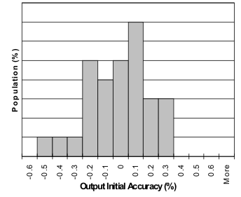 Figure 5. Output Voltage and Initial Accuracy (210°C)
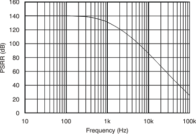 Figure 7. Power-Supply Rejection Ratio vs Frequency
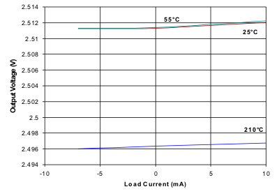 Figure 9. Output Voltage vs Load Current
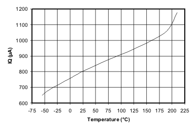
 Figure 11. Quiescent Current vs Temperature
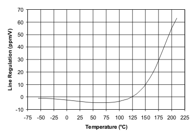 Figure 13. Line Regulation vs Temperature
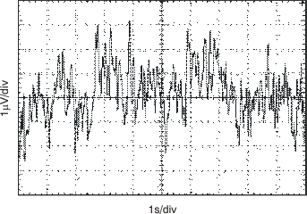 Figure 15. Noise
 Figure 17. Start-Up (REF5025)
 Figure 19. Load Transient
 Figure 21. Load Transient
 Figure 23. Line Transient

 Figure 2. Temperature Drift (0°C to 85°C)
 Figure 4. Temperature Drift (–55°C to +210°C)
 Figure 6. Output Voltage Accuracy vs Temperature
 Figure 8. Dropout Voltage vs Load Current
 Figure 10. Temperature Pin Output Voltage vs Temperature
 Figure 12. Quiescent Current vs Input Voltage
 Figure 14. Short-Circuit Current vs Temperature


 Figure 3. Temperature Drift (–40°C to +125°C)
 Figure 5. Output Voltage and Initial Accuracy (210°C)
 Figure 7. Power-Supply Rejection Ratio vs Frequency
 Figure 9. Output Voltage vs Load Current
 Figure 13. Line Regulation vs Temperature
 Figure 15. Noise
