ZHCSF43B May   2016  – August 2016 REF6025 , REF6030 , REF6033 , REF6041 , REF6045 , REF6050

PRODUCTION DATA.  

  1. 特性
  2. 应用
  3. 说明
  4. 修订历史记录
  5. Device Comparison Table
  6. Pin Configuration and Functions
  7. Specifications
    1. 7.1 Absolute Maximum Ratings
    2. 7.2 ESD Ratings
    3. 7.3 Recommended Operating Conditions
    4. 7.4 Thermal Information
    5. 7.5 Electrical Characteristics
    6. 7.6 Typical Characteristics
  8. Parameter Measurement Information
    1. 8.1 Solder Heat Shift
    2. 8.2 Thermal Hysteresis
    3. 8.3 Reference Droop Measurements
    4. 8.4 1/f Noise Performance
  9. Detailed Description
    1. 9.1 Overview
    2. 9.2 Functional Block Diagram
    3. 9.3 Feature Description
      1. 9.3.1 Integrated ADC Drive Buffer
      2. 9.3.2 Temperature Drift
      3. 9.3.3 Load Current
      4. 9.3.4 Stability
    4. 9.4 Device Functional Modes
  10. 10Applications and Implementation
    1. 10.1 Application Information
    2. 10.2 Typical Application
      1. 10.2.1 Design Requirements
      2. 10.2.2 Detailed Design Procedure
        1. 10.2.2.1 Results
      3. 10.2.3 Application Curves
  11. 11Power Supply Recommendations
  12. 12Layout
    1. 12.1 Layout Guidelines
    2. 12.2 Layout Example
  13. 13器件和文档支持
    1. 13.1 文档支持
      1. 13.1.1 相关文档 
    2. 13.2 相关链接
    3. 13.3 接收文档更新通知
    4. 13.4 社区资源
    5. 13.5 商标
    6. 13.6 静电放电警告
    7. 13.7 Glossary
  14. 14机械、封装和可订购信息

封装选项

机械数据 (封装 | 引脚)
散热焊盘机械数据 (封装 | 引脚)
订购信息

12 Layout

12.1 Layout Guidelines

Figure 62 illustrates an example of a PCB layout for a data-acquisition system using the REF60xx. Some key considerations are:

  • Connect low-ESR, 0.1-μF ceramic bypass capacitors between the VIN pin and ground.
  • Place the REF60xx output capacitor (CL) and the ADC as close to each other as possible.
  • Run two separate traces between VOUT_F, VOUT_S and the output capacitor, as shown in Figure 62.
  • Short the GND_F and GND_S pins with a solid plane, and extend this plane to connect to the output capacitor CL, as shown in Figure 62.
  • Use a solid ground plane to help distribute heat and reduces electromagnetic interference (EMI) noise pickup.
  • Place the external components as close to the device as possible. This configuration prevents parasitic errors (such as the Seebeck effect) from occurring.
  • Do not run sensitive analog traces in parallel with digital traces. Avoid crossing digital and analog traces if possible, and only make perpendicular crossings when absolutely necessary.

12.2 Layout Example
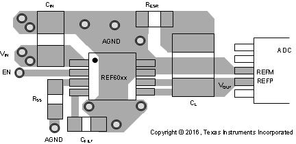
REF6025 REF6030 REF6033 REF6041 REF6045 REF6050 Layout_REF60xx_BOS708.gif Figure 62. Layout Example