ZHCSFI5 September   2016 REF6225 , REF6230 , REF6233 , REF6241 , REF6245 , REF6250

PRODUCTION DATA.  

  1. 特性
  2. 应用
  3. 说明
  4. Device Comparison Table
  5. Pin Configuration and Functions
  6. Specifications
    1. 6.1 Absolute Maximum Ratings
    2. 6.2 ESD Ratings
    3. 6.3 Recommended Operating Conditions
    4. 6.4 Thermal Information
    5. 6.5 Electrical Characteristics
    6. 6.6 Typical Characteristics
  7. Parameter Measurement Information
    1. 7.1 Solder Heat Shift
    2. 7.2 Thermal Hysteresis
    3. 7.3 Reference Droop Measurements
    4. 7.4 1/f Noise Performance
  8. Detailed Description
    1. 8.1 Overview
    2. 8.2 Functional Block Diagram
    3. 8.3 Feature Description
      1. 8.3.1 Integrated ADC Drive Buffer
      2. 8.3.2 Temperature Drift
      3. 8.3.3 Load Current
      4. 8.3.4 Stability
    4. 8.4 Device Functional Modes
  9. Applications and Implementation
    1. 9.1 Application Information
    2. 9.2 Typical Application
      1. 9.2.1 Design Requirements
      2. 9.2.2 Detailed Design Procedure
        1. 9.2.2.1 Results
      3. 9.2.3 Application Curves
  10. 10Power Supply Recommendations
  11. 11Layout
    1. 11.1 Layout Guidelines
    2. 11.2 Layout Example
  12. 12器件和文档支持
    1. 12.1 文档支持
      1. 12.1.1 相关文档 
    2. 12.2 相关链接
    3. 12.3 接收文档更新通知
    4. 12.4 社区资源
    5. 12.5 商标
    6. 12.6 静电放电警告
    7. 12.7 Glossary
  13. 13机械、封装和可订购信息

封装选项

机械数据 (封装 | 引脚)
散热焊盘机械数据 (封装 | 引脚)
订购信息

Power Supply Recommendations

The REF62xx family of references have extremely low dropout voltage. The dropout specifications can be found in the Electrical Characteristics section. A minimum 0.1 µF decoupling capacitor must be connected between the VIN and GND_F pins of the REF62xx. A typical dropout voltage versus load is shown in Figure 60.
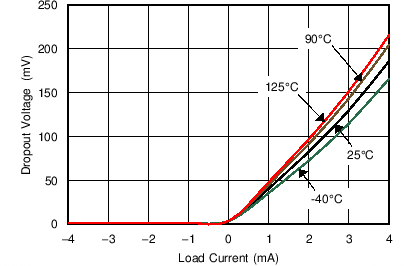
REF6225 REF6230 REF6233 REF6241 REF6245 REF6250 C017_SBOS708.png
Figure 60. Dropout Voltage vs Load Current