ZHCSM80G October 2020 – September 2023 REF70
PRODMIX
- 1
- 1 特性
- 2 应用
- 3 说明
- 4 Revision History
- 5 Device Comparison Table
- 6 Pin Configuration and Functions
-
7 Specifications
- 7.1 Absolute Maximum Ratings
- 7.2 ESD Ratings
- 7.3 Recommended Operating Conditions
- 7.4 Thermal Information
- 7.5 REF7012 Electrical Characteristics
- 7.6 REF7025 Electrical Characteristics
- 7.7 REF7030 Electrical Characteristics
- 7.8 REF7033 Electrical Characteristics
- 7.9 REF7040 Electrical Characteristics
- 7.10 REF7050 Electrical Characteristics
- 7.11 Typical Characteristics
- 8 Parameter Measurement Information
- 9 Detailed Description
- 10Application and Implementation
- 11Device and Documentation Support
- 12Mechanical, Packaging, and Orderable Information
8.1 Solder Heat Shift
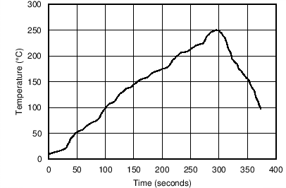
The materials used in the manufacture of the REF70 have differing coefficients of thermal expansion, resulting in stress on the device die when the part is heated during soldering process. Mechanical and thermal stress on the device die can cause the output voltages to shift, degrading the initial accuracy specifications of the product. Reflow soldering is a common cause of this error. In order to illustrate this effect, a total of 32 devices were soldered on two printed circuit boards [16 devices on each printed circuit board (PCB)] using lead-free solder paste and the paste manufacturer suggested reflow profile. The reflow profile is as shown in Figure 8-1. The printed circuit board is comprised of FR4 material. The board thickness is 1.65 mm and the area is 114 mm × 152 mm.
For recommended reflow profiles using 'Sn-Pb Eutectic Assembly' or 'Pb-Free Assembly' please refer JEDEC J-STD-020 standard.
 Figure 8-1 Reflow Profile
The reference output voltage is measured before and after the reflow process. Although all tested units exhibit very low shifts, higher shifts are also possible depending on the size, thickness, and material of the printed circuit board. An important note is that the Figure 8-2 and Figure 8-3 display the typical shift for exposure to a single reflow profile. Exposure to multiple reflows, as is common on PCBs with surface-mount components on both sides, causes additional shifts in the output bias voltage. If the PCB is exposed to multiple reflows, the device must be soldered in the last pass to minimize its exposure to thermal stress.
 Figure 8-2 Solder Shift (LCCC
Package)
 Figure 8-3 Solder Shift (VSSOP
Package)