ZHCSB37C November 2012 – November 2014 RF430CL330H
PRODUCTION DATA.
- 1器件概述
- 2修订历史记录
- 3Terminal Configuration and Functions
-
4Specifications
- 4.1 Absolute Maximum Ratings
- 4.2 Handling Ratings
- 4.3 Recommended Operating Conditions
- 4.4 Recommended Operating Conditions, Resonant Circuit
- 4.5 Supply Currents
- 4.6 Digital Inputs
- 4.7 Digital Outputs
- 4.8 Thermal Characteristics
- 4.9 Serial Communication Protocol Timings
- 4.10 I2C Interface
- 4.11 SPI Interface
- 4.12 RF143B, Recommended Operating Conditions
- 4.13 RF143B, ISO14443B ASK Demodulator
- 4.14 RF143B, ISO14443B-Compliant Load Modulator
- 4.15 RF143B, Power Supply
- 5Detailed Description
- 6器件和文档支持
- 7机械封装和可订购信息
封装选项
机械数据 (封装 | 引脚)
散热焊盘机械数据 (封装 | 引脚)
- RGT|16
订购信息
5 Detailed Description
5.1 Functional Block Diagram
Figure 5-1 shows the functional block diagram.
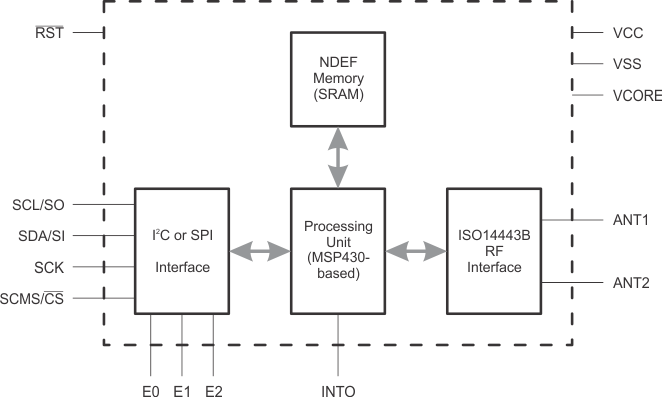 Figure 5-1 Functional Block Diagram
5.2 Serial Communication Interface
A "dual-mode" serial communication interface supports either SPI or I2C communication. The serial interface allows writing and reading the internal NDEF memory as well as configuring the device operation.
5.3 SPI or I2C Mode Selection
The selection between I2C or SPI mode takes place during the power-up and initialization phase of the device based on the input level at pin SCMS/CS (see Table 5-1).
Table 5-1 SPI or I2C Mode Selection
| Input Level at SCMS/CS During Initialization | Selected Serial Interface |
|---|---|
| 0 | I2C |
| 1 | SPI |
During initialization, an integrated pullup resistor pulls SCMS/CS high, which makes SPI the default interface. To enable I2C, this pin must be tied low externally. The pullup resistor is disabled after initialization to avoid any current through the resistor during normal operation. In SPI mode, the pin reverts to its CS functionality after initialization.
5.4 Communication Protocol
The tag is programmed and controlled by writing data into and reading data from the address map shown in Table 5-2 via the serial interface (SPI or I2C).
Table 5-2 User Address Map
| Range | Address | Size | Description |
|---|---|---|---|
| Registers | 0xFFFE | 2B | Control Register |
| 0xFFFC | 2B | Status Register | |
| 0xFFFA | 2B | Interrupt Enable | |
| 0xFFF8 | 2B | Interrupt Flags | |
| 0xFFF6 | 2B | CRC Result (16-bit CCITT) | |
| 0xFFF4 | 2B | CRC Length | |
| 0xFFF2 | 2B | CRC Start Address | |
| 0xFFF0 | 2B | Communication Watchdog Control Register | |
| 0xFFEE | 2B | Version | |
| 0xFFEC | 2B | Reserved | |
| 0xFFEA | 2B | Reserved | |
| 0xFFE8 | 2B | Reserved | |
| 0xFFE6 | 2B | Reserved | |
| 0xFFE4 | 2B | Reserved | |
| 0xFFE2 | 2B | Reserved | |
| 0xFFE0 | 2B | Reserved | |
| Reserved | 0x4000 to 0xFFDF | Reserved | |
| 0x0C00 to 0x3FFF | 13KB | Reserved (for example, future extension of NDEF Memory size) | |
| NDEF | 0x0000 to 0x0BFF | 3KB | NDEF Memory |
NOTE
Crossing Range Boundaries
Crossing range boundaries causes writes to be ignored and reads to return undefined data.
5.5 I2C Protocol
A command is always initiated by the master by addressing the device using the specified I2C device address. The device address is a 7-bit I2C address. The upper 4 bits are hard-coded, and the lower 3 bits are programmable by the input pins E0 through E2.
Table 5-3 I2C Device Address
| Bit 6 | Bit 5 | Bit 4 | Bit 3 | Bit 2 | Bit 1 | Bit 0 |
| 0 | 1 | 0 | 1 | E2 | E1 | E0 |
| MSB | LSB |
To write data, the device is addressed using the specified I2C device address with R/W = 0, followed by the upper 8 bits of the first address to be written and the lower 8 bits of that address. Next (without a repeated start), the data to be written starting at the specified address is received. With each data byte received, the address is automatically incremented by 1. The write access is terminated by the STOP condition on the I2C bus.
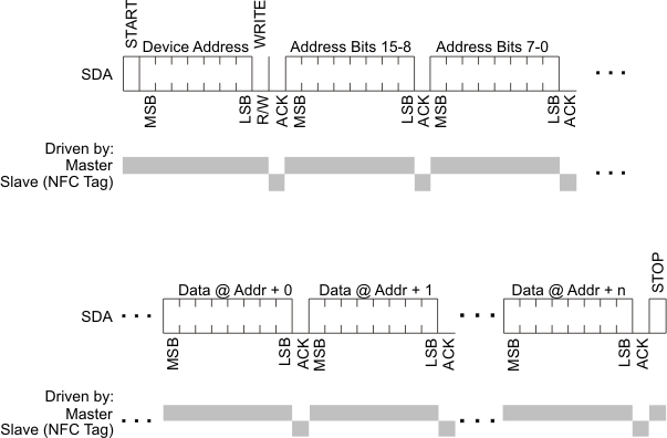 Figure 5-2 I2C Write Access
To read data, the device is addressed using the specified I2C device address with R/W = 0, followed by the upper 8 bits of the first address to be read and then the lower 8 bits of that address. Next, a repeated start condition is expected with the I2C device address and R/W = 1. The device then transmit data starting at the specified address until a non-acknowledgment and a STOP condition is received.
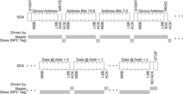 Figure 5-3 I2C Read Access
The following figures show examples of I2C accesses to the Control register at address 0xFFFE.
 Figure 5-4 I2C Access Example: Write of the Control Register at Address 0xFFFE With 0x00, 0x02 (RF Enable = 1)
 Figure 5-5 I2C Access Example: Read of the Control Register at Address 0xFFFE, Responds With 0x00, 0x02 (RF Enable = 1)
5.5.1 BIP-8 Communication Mode With I2C
The BIP-8 communication mode is enabled by setting the BIP-8 bit in the General Control register. All communication after setting this bit uses the following conventions with exactly 2 address bytes (16-bit address) and 2 data bytes (16-bit data).
Table 5-4 Write Access
| Master | Address Bits 15 to 8 |
Address Bits 7 to 0 |
Data at Addr + 0 | Data at Addr + 1 | BIP-8 |
| Slave | n/a | n/a | n/a | n/a | n/a |
The Bit-Interleaved Parity (BIP-8) is calculated using 16-bit address and 16-bit data. If the received BIP-8 does not match with received data no write will be performed. (The BIP-8 calculation does not include the I2C device address).
Table 5-5 Read Access
| Master | Address Bits 15 to 8 |
Address Bits 7 to 0 |
n/a | n/a | n/a |
| Slave | n/a | n/a | Data at Addr + 0 | Data at Addr + 1 | BIP-8 |
For read access, the Bit-Interleaved Parity (BIP-8) is calculated using the received 16-bit address and the 2 transmitted data bytes, and it is transmitted back to the master. The BIP-8 does not include the device address.
5.6 SPI Protocol
The SPI communication mode (SCK idle state and clock phase) is selected by tying E0 and E1 to VSS or VCC according to Table 5-6.
Table 5-6 SPI Mode Selection
| E1 | E0 | SPI Mode |
|---|---|---|
| 0 | 0 |
SPI Mode 0 with CPOL = 0 and CPHA = 0 SCK idle state: 0 |
| 0 | 1 |
SPI Mode 1 with CPOL = 0 and CPHA = 1 SCK idle state: 0 |
| 1 | 0 |
SPI Mode 2 with CPOL = 1 and CPHA = 0 SCK idle state: 1 |
| 1 | 1 |
SPI Mode 3 with CPOL = 1 and CPHA = 1 SCK idle state: 1 |
An SPI communication is always initiated by the master by pulling the CS pin low.
To write data into the device, this is followed by the master sending a write command (0x02) followed by the upper 8 bits of the first address to be written and then the lower 8 bits of that address. Next, the data to be written starting at the specified address is received. With each data byte received, the address is automatically incremented by 1. The write access is terminated by pulling the CS pin high.
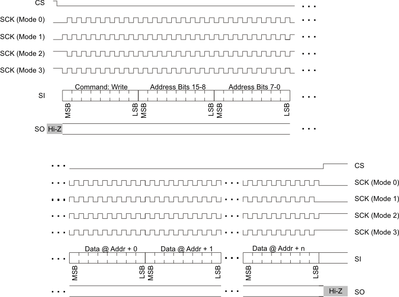 Figure 5-6 SPI Write Access
To read data from the device, pulling the CS pin low is followed by the master sending a read command (0x03 or 0x0B) followed by the upper 8 bits of the first address to be read, the lower 8 bits of that address, and a dummy byte. The device responds with the data that is read starting at the specified address until the CS pin is pulled high.
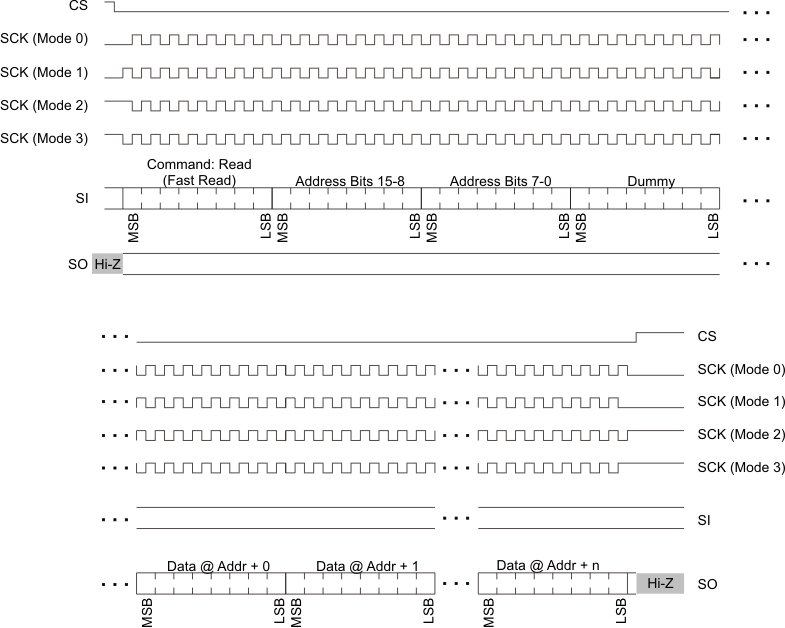 Figure 5-7 SPI Read Access (Command: 0x03 or 0x0B)
Commands other than write (0x02) and read (0x03 or 0x0B) are ignored. There is no difference in using the read command 0x03 or 0x0B.
Figure 5-8 and Figure 5-9 show examples of SPI accesses to the Control register at address 0xFFFE.
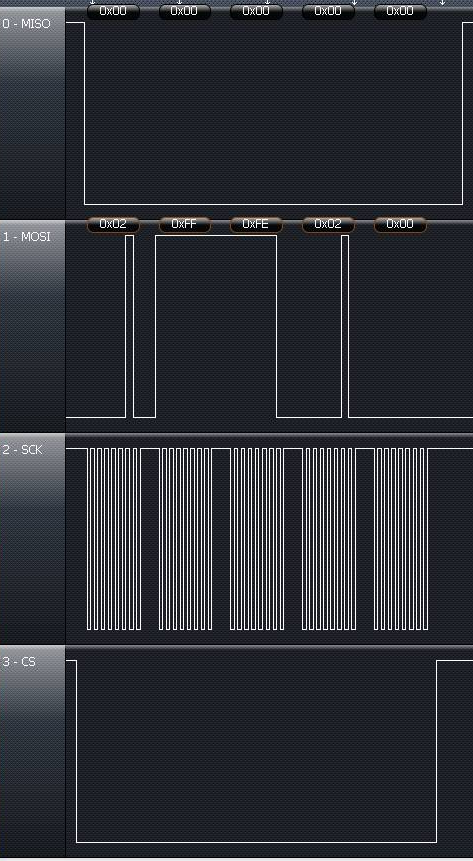 Figure 5-8 SPI Access Example: Write of the Control Register at Address 0xFFFE With 0x00, 0x02 (RF Enable = 1)
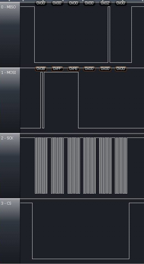 Figure 5-9 SPI Access Example: Read of the Control Register at Address 0xFFFE, Responds With 0x00, 0x02 (RF Enable = 1)
5.6.1 BIP-8 Communication Mode With SPI
The BIP-8 communication mode is enabled by setting the BIP-8 bit in the General Control register. All communication after setting this bit uses the following conventions with exactly 2 address bytes (16-bit address) and 2 data bytes (16-bit data).
Table 5-7 Write Access
| SI | Command: Write | Address Bits 15 to 8 |
Address Bits 7 to 0 |
Data at Addr + 0 | Data at Addr + 1 | BIP-8 |
| SO | n/a | n/a | n/a | n/a | n/a | n/a |
The Bit-Interleaved Parity (BIP-8) is calculated using 16-bit address and 16-bit data. If the received BIP-8 does not match with received data no write will be performed. (The BIP-8 calculation does not include the write-command byte.)
Table 5-8 Read Access
| SI | Command: Read | Address Bits 15 to 8 |
Address Bits 7 to 0 |
Dummy Byte | n/a | n/a | n/a |
| SO | n/a | n/a | n/a | n/a | Data at Addr + 0 | Data at Addr + 1 | BIP-8 |
For read access the Bit-Interleaved Parity (BIP-8) is calculated using the received 16-bit address, the received dummy byte and the 2 transmitted data bytes and transmitted back to the master. It does not include the read-command byte.
5.7 Registers
NOTE
Endianness
All 16-bit registers are little-endian: the least significant byte with bits 7-0 is at the lowest address (and this address is always even). The most significant byte with bits 15-8 is at the highest address (always odd).
5.7.1 General Control Register
Table 5-9 General Control Register
| Addr: | 15 | 14 | 13 | 12 | 11 | 10 | 9 | 8 |
| 0xFFFF | Reserved | |||||||
| Addr: | 7 | 6 | 5 | 4 | 3 | 2 | 1 | 0 |
| 0xFFFE | Reserved | Standby Enable | BIP-8 | INTO Drive | INTO High | Enable INT | Enable RF | SW-Reset |
Table 5-10 General Control Register Description
| Bit | Field | Type | Reset | Description |
|---|---|---|---|---|
| 0 | SW-Reset | W | 0 |
0b = Always reads 0. 1b = Resets the device to default settings and clears memory. The serial communication is restored after tReady, and the register settings and NDEF memory must be restored afterward. |
| 1 | Enable RF | R/W | 0 |
Global enable of RF interface. The RF interface should be disabled when writing to the NDEF memory. Enabling the RF interface triggers a basic check of the NDEF structure. If this check fails, the RF interface remains disabled and the NDEF Error interrupt flag is set. When the RF interface is enabled, writes using the serial interface (except to disable the RF interface) are discouraged to avoid any interference with RF communication. 0b = RF interface disabled 1b = RF interface enabled |
| 2 | Enable INT | R/W | 0 |
Global Interrupt Output Enable 0b = Interrupt output disabled. The INTO pin is Hi-Z. 1b = Interrupt output enabled. The INTO pin signals any enabled interrupt according to the INTO High and INTO Drive bits. |
| 3 | INTO High | R/W | 0 |
Interrupt Output pin INTO Configuration 0b = Interrupts are signaled with an active low 1b = Interrupts are signaled with an active high |
| 4 | INTO Drive | R/W | 0 |
Interrupt Output pin INTO Configuration 0b = Pin is Hi-Z if there is no pending interrupt. Application provides an external pullup resistor if bit 3 (INTO Active High) = 0. Application provides an external pulldown resistor if bit 3 (INTO Active High) = 1. 1b = Pin is actively driven high or low if there is no pending interrupt. It is driven high if bit 3 (INTO Active High) = 0. It is driven low if bit 3 (INTO Active High) = 1. |
| 5 | BIP-8 | R/W | 0 |
Enables BIP-8 communication mode (bit interleaved parity). If BIP-8 is enabled, a separate running tally is kept of the parity (that is, the number of ones that occur) for every bit position in the bytes included in the BIP-8 calculation. The corresponding bit position of the BIP-8 byte is set to 1 if the parity is currently odd and is set to 0 if the parity is even – resulting in an overall even parity for each bit position including the BIP-8 byte. All communication when this bit is set must follow the conventions defined in the BIP-8 communication mode sections for I2C and SPI. 0b = BIP-8 communication mode disabled 1b = BIP-8 communication mode enabled |
| 6 | Standby Enable | R/W | 0 |
Enables a low-power standby mode. The standby mode is entered if the RF interface is disabled, the communication watchdog is disabled, and no serial communication is ongoing. 0b = Standby mode disabled 1b = Standby mode enabled |
| 7 | Reserved | R/W | 0 | |
| 8-15 | Reserved | R | 0 |
5.7.2 Status Register
Table 5-11 Status Register
| Addr: | 15 | 14 | 13 | 12 | 11 | 10 | 9 | 8 |
| 0xFFFD | Reserved | |||||||
| Addr: | 7 | 6 | 5 | 4 | 3 | 2 | 1 | 0 |
| 0xFFFC | Reserved | RF Busy | CRC Active | NDEF Ready | ||||
Table 5-12 Status Register Description
| Bit | Field | Type | Reset | Description |
|---|---|---|---|---|
| 0 | Ready | R | 0 |
0b = Device not ready to receive updates to the NDEF memory from the serial interface. 1b = Device ready. NDEF memory can be written by the serial interface. |
| 1 | CRC Active | R | 0 |
0b = No CRC calculation ongoing 1b = CRC calculation ongoing |
| 2 | RF Busy | R | 0 |
0b = No RF communication ongoing 1b = RF communication ongoing |
| 3-15 | Reserved | R | 0 |
5.7.3 Interrupt Registers
The interrupt enable register (see Table 5-13 and Table 5-14) determines which interrupt events are signaled on the external output pin INTO. Setting any bit high in this register allows the corresponding event to trigger the interrupt signal. See Table 5-17 for a description of each interrupt.
All enabled interrupt signals are ORed together, and the result is signaled on the output pin INTO.
Table 5-13 Interrupt Enable Register
| Addr: | 15 | 14 | 13 | 12 | 11 | 10 | 9 | 8 |
| 0xFFFB | Reserved | |||||||
| Addr: | 7 | 6 | 5 | 4 | 3 | 2 | 1 | 0 |
| 0xFFFA | Generic Error | Reserved | NDEF Error | BIP-8 Error Detected | CRC Calculation Completed | End of Write | End of Read | Reserved |
Table 5-14 Interrupt Enable Register Description
| Bit | Field | Type | Reset | Description |
|---|---|---|---|---|
| 0-15 | Interrupt Enables | R/W | 0 |
Enable for the corresponding IRQ. All enabled interrupt signals are ORed together, and the result is signaled on the output pin INTO. 0b = IRQ disabled 1b = IRQ enabled |
The interrupt flag register (see Table 5-15 and Table 5-16) is used to report the status of any interrupts that are pending. Setting any bit high in this register acknowledges and clears the interrupt associated with the respective bit. See Table 5-17 for a description of each interrupt.
Table 5-15 Interrupt Flag Register
| Addr: | 15 | 14 | 13 | 12 | 11 | 10 | 9 | 8 |
| 0xFFF9 | Reserved | |||||||
| Addr: | 7 | 6 | 5 | 4 | 3 | 2 | 1 | 0 |
| 0xFFF8 | Generic Error | Reserved | NDEF Error | BIP-8 Error Detected | CRC Calculation Completed | End of Write | End of Read | Reserved |
Table 5-16 Interrupt Flag Register Description
| Bit | Field | Type | Reset | Description |
|---|---|---|---|---|
| 0-15 | Interrupt Flags | R/W | 0 |
Flag pending IRQ. Read Access: 0b = No pending IRQ. 1b = Pending IRQ. Write Access: 0b = No change. 1b = Clear pending IRQ flag. |
Table 5-17 Interrupts
| Bit | Field | Description |
|---|---|---|
| 0 | Reserved | |
| 1 | End of Read |
This IRQ occurs when the RF field is turned off by the reader after the reader has performed a read of the NDEF message. |
| 2 | End of Write |
This IRQ occurs when the RF field is turned off by the reader after the reader has performed a write into the NDEF message. |
| 3 | CRC Calculation Completed |
This IRQ occurs when a CRC calculation that is triggered by writing into the CRC registers is completed and the result can be read from the CRC result register (see Section 5.7.4). |
| 4 | BIP-8 Error Detected |
This IRQ occurs when a BIP-8 error is detected (only if the BIP-8 communication mode is enabled). |
| 5 | NDEF Error | This IRQ occurs if an error is detected in the NDEF structure after an attempt to enable the RF interface. |
| 6 | Reserved | |
| 7 | Generic Error |
This IRQ occurs for any error that makes the device unreliable or non-operational. |
| 8-15 | Reserved |
5.7.4 CRC Registers
Writing the CRC address and the CRC length registers initiates a 16-bit CRC calculation of the specified address range. The length is always assumed to be even (16-bit aligned). Writing the length register starts the CRC calculation.
During the CRC calculation, the CRC active bit is set (=1). When the calculation is complete, the "CRC completion" interrupt flag is set and the result of the CRC calculation can be read from the CRC result register. It is recommended to perform a CRC calculation only when the RF interface is disabled (RF Enable = 0).
Table 5-18 CRC Result Register
| Addr: | 15 | 14 | 13 | 12 | 11 | 10 | 9 | 8 |
| 0xFFF7 | CRC CCITT Result (high byte) | |||||||
| Addr: | 7 | 6 | 5 | 4 | 3 | 2 | 1 | 0 |
| 0xFFF6 | CRC CCITT Result (low byte) | |||||||
Table 5-19 CRC Result Register Description
| Bit | Field | Type | Reset | Description |
|---|---|---|---|---|
| 0-15 | CRC-CCITT Result | R | 0 | CRC-CCITT Result |
Table 5-20 CRC Length Register
| Addr: | 15 | 14 | 13 | 12 | 11 | 10 | 9 | 8 |
| 0xFFF5 | CRC Length (high byte) | |||||||
| Addr: | 7 | 6 | 5 | 4 | 3 | 2 | 1 | 0 |
| 0xFFF4 | CRC Length (low byte) | |||||||
Table 5-21 CRC Length Register Description
| Bit | Field | Type | Reset | Description |
|---|---|---|---|---|
| 0-15 | CRC Length | RW | 0 | CRC Length - always assumed to be even (Bit 0 = 0). Writing into high byte starts CRC calculation. |
Table 5-22 CRC Start Address Register
| Addr: | 15 | 14 | 13 | 12 | 11 | 10 | 9 | 8 |
| 0xFFF3 | CRC Start Address (high byte) | |||||||
| Addr: | 7 | 6 | 5 | 4 | 3 | 2 | 1 | 0 |
| 0xFFF2 | CRC Start Address (low byte) | |||||||
Table 5-23 CRC Start Address Register Description
| Bit | Field | Type | Reset | Description |
|---|---|---|---|---|
| 0-15 | CRC Start Address | RW | 0 | CRC Start Address. Defines start address within NDEF memory. This address is always assumed to be even (bit 0 = 0). |
The CRC is calculated based on the CCITT polynomial initialized with 0xFFFF.
CCITT polynomial: x16 + x12 + x5 + 1
5.7.5 Communication Watchdog Register
When the communication watchdog is enabled, it expects a write or read access within a specified period; otherwise, the watchdog resets the device. If the BIP-8 communication mode is enabled, the transfer must be valid to be accepted as a watchdog reset.
Table 5-24 Communication Watchdog Register
| Addr: | 15 | 14 | 13 | 12 | 11 | 10 | 9 | 8 |
| 0xFFF1 | Reserved | |||||||
| Addr: | 7 | 6 | 5 | 4 | 3 | 2 | 1 | 0 |
| 0xFFF0 | Reserved | Timeout Period Selection | Enable | |||||
Table 5-25 Communication Watchdog Register Description
| Bit | Field | Type | Reset | Description |
|---|---|---|---|---|
| 0 | Enable | R/W | 0 |
0b = Communication Watchdog disabled 1b = Communication Watchdog enabled |
| 1 | Timeout Period Selection | R/W | 0 |
000b = 2 s ± 30%(1) 001b = 32 s ± 30%(1) 010b = 8.5 min ± 30%(1) 011b to 111b = Reserved |
| 4-15 | Reserved | R | 0 |
5.7.6 Version Registers
Provides version information about the implemented ROM code.
Table 5-26 Version Register
| Addr: | 15 | 14 | 13 | 12 | 11 | 10 | 9 | 8 |
| 0xFFEF | Software Version | |||||||
| Addr: | 7 | 6 | 5 | 4 | 3 | 2 | 1 | 0 |
| 0xFFEE | Software Identification | |||||||
Table 5-27 Version Register Description
| Bit | Field | Type | Reset | Description |
|---|---|---|---|---|
| 0-7 | Software Identification | R |
0x01: RF430CL330H Firmware |
|
| 8-15 | Software Version | R |
Software version |
5.8 NFC Type-4 Tag Functionality
This device is an ISO14443B-compliant transponder that operates according to the NFC Forum Tag Type-4 specification and supports the NFC Forum NDEF (NFC Data Exchange Format) requirements. Through the RF interface, the user can read and update the contents in the NDEF memory. The contents in the NDEF memory (stored in SRAM) are stored as long as power is maintained.
NOTE
This device does not have nonvolatile memory; therefore, the information stored in the NDEF memory is lost when power is removed.
This device does not support the peer-to-peer or reader/writer modes in the ISO18092/NFC Forum specification. All RF communication between an NFC forum device and this device is in the passive tag mode. The device responds by load modulation and is not considered an intentional radiator.
This device is intended to be used in applications where the primary reader/writer is for example an NFC-enabled cell phone. The device enables data transfer to and from an NFC phone by RF to the host application that is enabled with the dual interface device. In this case, the host application can be considered the destination device, and the cell phone or other type of mobile device is treated as the end-point device.
This device supports ISO14443-3, ISO14443-4, and NFC Forum commands as described in the following sections. A high-level overview of the ISO14443B and NFC commands and responses are shown in Figure 5-10.
106-kbps, 212-kbps, 424-kbps, and 848-kbps data rates are supported.
The device always answers ATTRIB commands from the PCD that request higher data rates. Note, this is not NFC-compliant, because for NFC-B the maximum data rate specified is 106 kbps. It is assumed that an NFC-compliant PCD would not request higher data rates thus no interoperability issues are expected.
Even though all data rates up to 848 kbps are supported, the device by default reports only the capability to support 106 kbps to the PCD. To change this behavior, use the sequence described in Section 5.8.3.
The ISO14443B command and response structure is detailed in ISO14443-3, ISO14443-4, and NFC Forum-TS-Digital Protocol. The applicable ISO7816-4 commands are detailed in NFC Forum-TS-Type-4-Tag_2.0.
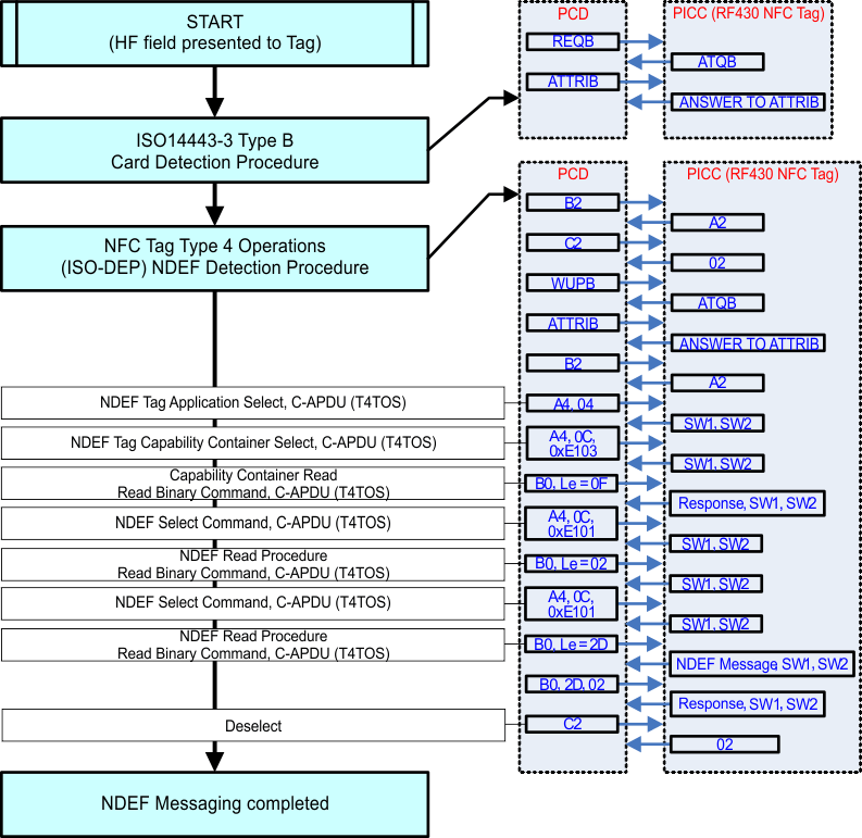 Figure 5-10 Command and Response Exchange Flow
5.8.1 ISO14443-3 Commands
These commands use the character, frame format, and timing that are described in ISO14443-3, clause 7.1. The following commands are used to manage communication:
REQB and WUPB
The REQB and WUPB Commands sent by the PCD are used to probe the field for PICCs of Type B. In addition, WUPB is used to wake up PICCs that are in the HALT state. The number of slots N is included in the command as a parameter to optimize the anticollision algorithm for a given application.
Slot-MARKER
After a REQB or WUPB Command, the PCD may send up to (N-1) Slot-MARKER Commands to define the start of each timeslot. Slot-MARKER Commands can be sent after the end of an ATQB message received by the PCD to mark the start of the next slot or earlier if no ATQB is received (no need to wait until the end of a slot, if this slot is known to be empty).
ATTRIB
The ATTRIB Command sent by the PCD includes information required to select a single PICC. A PICC receiving an ATTRIB Command with its identifier becomes selected and assigned to a dedicated channel. After being selected, this PICC only responds to commands defined in ISO/IEC 14443-4 that include its unique CID.
HLTB
The HLTB Command is used to set a PICC in HALT state and stop responding to a REQB.
After answering to this command, the PICC ignores any commands except the WUPB.
5.8.2 NFC Tag Type 4 Commands
Select
Selection of applications or files
ReadBinary
Read data from file
UpdateBinary
Update (erase and write) data to file
5.8.3 Data Rate Settings
106-kbps, 212-kbps, 424-kbps, and 848-kbps data rates are supported by the device.
The device always answers ATTRIB commands from the PCD that request higher data rates. Note, this is not NFC-compliant, because for NFC-B the maximum data rate specified is 106 kbps. It is assumed that an NFC-compliant PCD would not request higher data rates thus no interoperability issues are expected.
Even though all data rates up to 848 kbps are supported, the device by default reports only the capability to support 106 kbps to the PCD.
To change this behavior, follow these steps using the selected serial interface (I2C or SPI):
- Read the version register.
- Use the version register content to select one of the following sequences:
- If "Software Identification" = 01h and "Software Version" = 01h, follow the sequence in Table 5-28.
- If "Software Identification" = 01h and "Software Version" = 02h , follow the sequence in Table 5-29.
- If you do not want to support all data rates up to 847 kbps, then change the Data Rate Capability byte (Data 0 of Step 3. Write Access) according to Table 5-30.
- Perform the steps in the following tables.
Table 5-28 Data Rate Setting Sequence (Version = 0101h)
| Access Type | Addr Bits 15 to 8 |
Addr Bits 7 to 0 |
Data 0 | Data 1 |
|---|---|---|---|---|
| 1. Write Access | 0xFF | 0xE0 | 0x4E | 0x00 |
| 2. Write Access | 0xFF | 0xFE | 0x80 | 0x00 |
| 3. Write Access | 0x2A | 0xA4 | 0xC4(1) | 0x00 |
| 4. Write Access | 0x28 | 0x14 | 0x00 | 0x00 |
| 5. Write Access | 0xFF | 0xE0 | 0x00 | 0x00 |
Table 5-29 Data Rate Setting Sequence (Version = 0201h)
| Access Type | Addr Bits 15 to 8 |
Addr Bits 7 to 0 |
Data 0 | Data 1 |
|---|---|---|---|---|
| 1. Write Access | 0xFF | 0xE0 | 0x4E | 0x00 |
| 2. Write Access | 0xFF | 0xFE | 0x80 | 0x00 |
| 3. Write Access | 0x2A | 0x7C | 0xC4(1) | 0x00 |
| 4. Write Access | 0x28 | 0x14 | 0x00 | 0x00 |
| 5. Write Access | 0xFF | 0xE0 | 0x00 | 0x00 |
Table 5-30 Data Rate Capability
| Data Rata Capability Byte | Description | |||||||
|---|---|---|---|---|---|---|---|---|
| b7 | b6 | b5 | b4 | b3 | b2 | b1 | b0 | |
| 0 | 0 | 0 | 0 | 0 | 0 | 0 | 0 | PICC supports only 106-kbps in both directions (default). |
| 1 | x | x | x | 0 | x | x | x | Same data rate from PCD to PICC and from PICC to PCD compulsory |
| x | x | x | 1 | 0 | x | x | x | PICC to PCD, data rate supported is 212 kbps |
| x | x | 1 | x | 0 | x | x | x | PICC to PCD, data rate supported is 424 kbps |
| x | 1 | x | x | 0 | x | x | x | PICC to PCD, data rate supported is 847 kbps |
| x | x | x | x | 0 | x | x | 1 | PCD to PICC, data rate supported is 212 kbps |
| x | x | x | x | 0 | x | 1 | x | PCD to PICC, data rate supported is 424 kbps |
| x | x | x | x | 0 | 1 | x | x | PCD to PICC, data rate supported is 847 kbps |
5.9 NDEF Memory
This device implements 3KB of SRAM memory that must be written with the NDEF Application data.
Table 5-31 shows the mandatory structure. The data can be accessed through the RF interface only after the NDEF memory is correctly initialized through the serial interface (I2C or SPI).
While writing into the NDEF memory, the RF interface must be disabled by clearing the Enable RF bit in the General Control register. After the NDEF memory is properly initialized, the RF interface can be enabled be setting the Enable RF bit in the General Control register to 1. When the RF interface is enabled, the basic NDEF structure is checked for correctness. If an error in the structure is detected, the NDEF Error IRQ is triggered, and the RF interface remains disabled (the Enable RF bit in the General Control register is cleared to 0).
If the NDEF application data must be modified through the serial interface after the RF interface is enabled, it is recommended to read the RF Busy bit in the Status register. If the RF interface is busy, defer disabling the RF interface until the RF transaction is completed (indicated by RF Busy bit = 0).
Figure 5-11 shows the recommended flow how to control the access to the NDEF memory.
The address range for the NDEF memory is 0x0000 to 0x0BFF.
Table 5-31 NDEF Application Data (Mandatory)
|
NDEF Application Selectable by Name = D2_7600_0085_0101h |
Capability Container Selectable by File ID = E103h |
2B - CCLen | |||
| 1B - Mapping version | |||||
| 2B - MLe = 000F9h | |||||
| 2B - MLc = 000F6h | |||||
| NDEF File Ctrl TLV | 1B - Tag = 04h | The NDEF file control TLV is mandatory | |||
| 1B - Len = 06h | |||||
| 6B - Val | 2B - File Identifier | ||||
| 2B - Max file size | |||||
| 1B - Read access | |||||
| 1B - Write access | |||||
|
NDEF File Selectable by File ID = xxyyh |
2B - Len | Mandatory NDEF file | |||
| xB - Binary NDEF file content | |||||
| yB - Unused if Len < Max file size in File Ctrl TLV | |||||
Table 5-32 NDEF Application Data (Includes Proprietary Sections)
|
NDEF Application Selectable by Name = D2_7600_0085_0101h |
Capability Container Selectable by File ID = E103h |
2B - CCLen | |||
| 1B - Mapping version | |||||
| 2B - MLe = 000F9h | |||||
| 2B - MLc = 000F6h | |||||
| NDEF File Ctrl TLV | 1B - Tag = 04h | The NDEF file control TLV is mandatory | |||
| 1B - Len = 06h | |||||
| 6B - Val | 2B - File Identifier | ||||
| 2B - Max file size | |||||
| 1B - Read access | |||||
| 1B - Write access | |||||
| Proprietary File Ctrl TLV (1) | 1B - Tag = 05h | Zero or more proprietary file control TLVs | |||
| 1B - Len = 06h | |||||
| 6B - Val | 2B - File Identifier | ||||
| 2B - Max file size | |||||
| 1B - Read access | |||||
| 1B - Write access | |||||
| ⋮ | |||||
| Proprietary File Ctrl TLV (N) | 1B - Tag = 05h | ||||
| 1B - Len = 06h | |||||
| 6B - Val | 2B - File Identifier | ||||
| 2B - Max file size | |||||
| 1B - Read access | |||||
| 1B - Write access | |||||
|
NDEF File Selectable by File ID = xxyyh |
2B - Len | Mandatory NDEF file | |||
| xB - Binary NDEF file content | |||||
| yB - Unused if Len < Max file size in File Ctrl TLV | |||||
|
Proprietary File (1) Selectable by File ID = xxyyh |
2B - Len | Optional proprietary file | |||
| xB - Binary proprietary file content | |||||
| yB - Unused if Len < Max file size in File Ctrl TLV | |||||
| ⋮ | |||||
|
Proprietary File (N) Selectable by File ID = xxyyh |
2B - Len | Optional proprietary file | |||
| xB - Binary proprietary file content | |||||
| yB - Unused if Len < Max file size in File Ctrl TLV | |||||
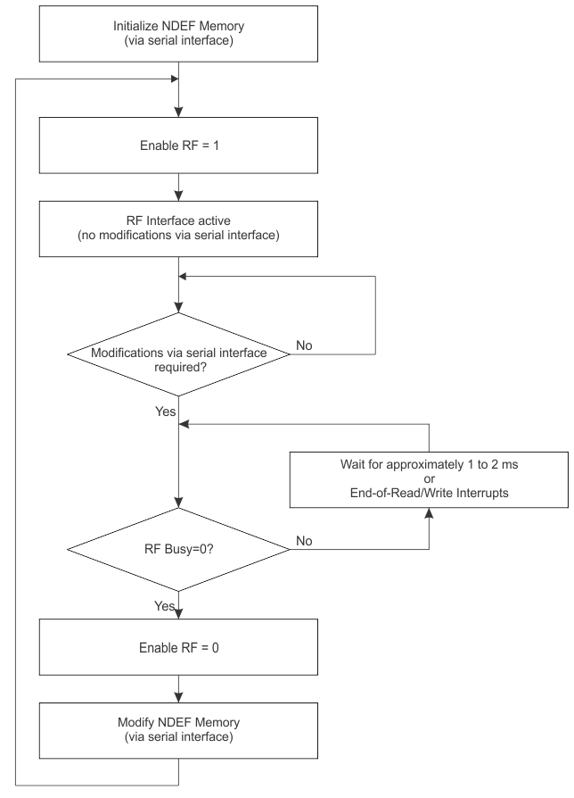 Figure 5-11 Recommended NDEF Memory Flow
5.9.1 NDEF Error Check
With the RF interface is enabled, the basic NDEF structure is automatically checked for correctness. If any of the following conditions are true, the error check fails, an NDEF error IRQ is triggered, and the RF interface remains disabled.
- CCLEN less than 0x000F or greater than 0xFFFE.
- MLe value is less than 0xF. Note, for best performance the MLe value should be programmed to 0x00F9.
- MLc is equal to zero. Note, for best performance the MLc value should be programmed to 0x00F6.
- TLV tag does not equal 0x4.
- TLV length does not equal 0x6.
- File ID equals 0, or 0xE102, or 0xE103, or 0x3F00, or 0x3FFF, or 0xFFFF.
- Max NDEF size is less than 0x5 or greater than 0xFFFE.
- Read access is greater than 0 and less than 0x80.
- Write Access is greater than 0 and less than 0x80.
Also the proprietary TLVs are checked. The check fails if any of the following conditions are true.
- TLV tag does not equal 0x05.
- TLV length does not equal 0x6.
- File ID equals 0, or 0xE102, or 0xE103, or 0x3F00, or 0x3FFF, or 0xFFFF.
- Max NDEF size is less than 0x5 or greater than 0xFFFE.
- Read access is greater than 0 and less than 0x80.
- Write Access is greater than 0 and less than 0x80.
5.10 Typical Usage Scenario
A typical usage scenario is as follows:
- Write capability container and messages into the NDEF memory (starting from address 0) using the serial interface.
- Enable interrupts (especially End of Read and End of Write).
- Configure the interrupt pin INTO as needed and enable the RF interface.
- Wait for interrupt signaled by INTO.
- Disable RF interface (but keep INTO settings unchanged).
- Read interrupt flag register to determine interrupt sources.
- Clear interrupt flags. INTO returns to inactive state.
- Read and modify NDEF memory as needed.
- Enable RF interface again (keeping INTO settings unchanged) and continue with (4).
5.11 References
ISO/IEC 14443-2: 2001, Part 2: Radio frequency interface power and signal interface
ISO/IEC 14443-3: 2001, Part 3: Initialization and anticollision
ISO/IEC 14443-4: 2001, Part 4: Transmission protocols
ISO/IEC 18092, NFC Communication Interface and Protocol-1 (NFCIP-1)
ISO/IEC 21481, NFC Communication Interface Protocol-2 (NFCIP-2)
NDEF NFC Forum Spec, NFC Data Exchange Format Specification