SNVS697E January 2011 – December 2016 SM72485
PRODUCTION DATA.
- 1 Features
- 2 Applications
- 3 Description
- 4 Revision History
- 5 Pin Configuration and Functions
- 6 Specifications
- 7 Detailed Description
- 8 Application and Implementation
- 9 Power Supply Recommendations
- 10Layout
- 11Device and Documentation Support
- 12Mechanical, Packaging, and Orderable Information
1 Features
- Operating Input Voltage: 6 V to 95 V
- Integrated 100-V, N-Channel Buck Switch
- Internal Start-Up Regulator
- No Loop Compensation Required
- Ultra-Fast Transient Response
- On-time Varies Inversely With Input Voltage
- Operating Frequency Remains Constant With Varying Line Voltage and Load Current
- Adjustable Output Voltage From 2.5 V
- Highly Efficient Operation
- Precision Internal Reference
- Low Bias Current
- Intelligent Current Limit
- Thermal Shutdown
- Package
- VSSOP (3 mm × 3 mm)
- WSON (4 mm × 4 mm)
2 Applications
- PV Panel Smart Junction Boxes
- Nonisolated Telecommunication Buck Regulator
- Secondary High Voltage Post Regulator
- 42-V Automotive Systems
3 Description
The SM72485 step-down switching regulator features all of the functions required to implement a low cost, efficient, Buck bias regulator. This high voltage regulator contains an 100-V N-channel buck switch. The device is easy to implement and is provided in the VSSOP and the thermally enhanced WSON package. The regulator is based on a control scheme using an on-time inversely proportional to VIN. This feature allows the operating frequency to remain relatively constant. The control scheme requires no loop compensation. An intelligent current limit is implemented with forced off-time, which is inversely proportional to VOUT. This scheme ensures short circuit control while providing minimum foldback. Other features include: Thermal shutdown, VCC undervoltage lockout, gate drive undervoltage lockout, maximum duty cycle limiter, and a precharge switch.
Device Information(1)
| PART NUMBER | PACKAGE | BODY SIZE (NOM) |
|---|---|---|
| SM72485 | VSSOP (8) | 3.00 mm × 3.00 mm |
| WSON (8) | 4.00 mm × 4.00 mm |
- For all available packages, see the orderable addendum at the end of the data sheet.
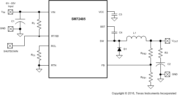
Typical Application, Basic Step-Down Regulator
