SNVS697E January 2011 – December 2016 SM72485
PRODUCTION DATA.
- 1 Features
- 2 Applications
- 3 Description
- 4 Revision History
- 5 Pin Configuration and Functions
- 6 Specifications
- 7 Detailed Description
- 8 Application and Implementation
- 9 Power Supply Recommendations
- 10Layout
- 11Device and Documentation Support
- 12Mechanical, Packaging, and Orderable Information
8 Application and Implementation
NOTE
Information in the following applications sections is not part of the TI component specification, and TI does not warrant its accuracy or completeness. TI’s customers are responsible for determining suitability of components for their purposes. Customers should validate and test their design implementation to confirm system functionality.
8.1 Application Information
The SM72485 is a step-down DC-to-DC regulator. It is typically used to convert a higher DC voltage to a lower DC voltage with a maximum output current of 150 mA. The following design procedure can be used to select components for the SM72485. This section presents a simplified discussion of the design process.
The final circuit is shown in Figure 10. The circuit was tested, and the resulting performance is shown in Figure 14 and Figure 15.
8.2 Typical Application
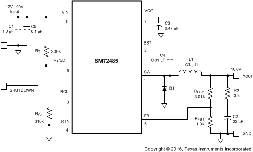 Figure 10. SM72485 Example Circuit Diagram
8.2.1 Design Requirements
For this design example, use the parameters listed in Table 1 as the input parameters.
Table 1. Design Parameters
| PARAMETER | EXAMPLE VALUE |
|---|---|
| Input voltage | 12 V to 90 V |
| Output voltage | 10 V |
| Minimum load current | 100 mA |
| Maximum load current | 150 mA |
| Feedback resistor ratio | 3:1 |
| Switching frequency | 234 kHz |
| Inductor | 200 µH |
8.2.2 Detailed Design Procedure
8.2.2.1 Selection of External Components
Here is a guide for determining the component values illustrated with a design example. See Functional Block Diagram and Table 2 for more information. The following sections configure the SM72485 for:
- Input voltage (VIN): 12 V to 90 V
- Output voltage (VOUT1): 10 V
- Load current (for continuous conduction mode): 100 mA to 150 mA
Table 2. Bill of Materials
| ITEM | DESCRIPTION | PART NUMBER | VALUE |
|---|---|---|---|
| C1 | Ceramic capacitor | TDK C4532X7R2A105M | 1 µF, 100 V |
| C2 | Ceramic capacitor | TDK C4532X7R1E226M | 22 µF, 25 V |
| C3 | Ceramic capacitor | Kemet C1206C474K5RAC | 0.47 µF, 50 V |
| C4 | Ceramic capacitor | Kemet C1206C103K5RAC | 0.01 µF, 50 V |
| C5 | Ceramic capacitor | TDK C3216X7R2A104M | 0.1 µF, 100 V |
| D1 | Schottky power diode | Diodes Inc. DFLS1100 | 100 V, 1 A |
| L1 | Power inductor | COILTRONICS DR125-221-R, or | 220 µH |
| TDK SLF10145T-221MR65 | |||
| RFB2 | Resistor | Vishay CRCW12063011F | 3.01 kΩ |
| RFB1 | Resistor | Vishay CRCW12061001F | 1 kΩ |
| R3 | Resistor | Vishay CRCW12063R30F | 3.3 Ω |
| RT | Resistor | Vishay CRCW12063093F | 309 kΩ |
| RCL | Resistor | Vishay CRCW12063163F | 316 kΩ |
| U1 | Switching regulator | Texas Instruments SM72485 | — |
8.2.2.1.1 RFB1 and RFB2
VOUT = VFB × (RFB1 + RFB2) / RFB1, and because VFB = 2.5 V, the ratio of RFB2 to RFB1 calculates as 3:1. Standard values of 3.01 kΩ and 1 kΩ are chosen. Other values could be used as long as the 3:1 ratio is maintained.
8.2.2.1.2 Fs and RT
The recommended operating frequency range for the SM72485 is 50 kHz to 1.1 MHz. Unless the application requires a specific frequency, the choice of frequency is generally a compromise, because it affects the size of L1 and C2, and the switching losses. The maximum allowed frequency, based on a minimum on-time of 400 ns, is calculated from Equation 6.
For this exercise, FMAX = 277 kHz. From Equation 2, RT calculates to 260 kΩ. A standard value 309-kΩ resistor is used to allow for tolerances in Equation 2, resulting in a frequency of 234 kHz.
8.2.2.1.3 L1
The main parameter affected by the inductor is the output current ripple amplitude. The choice of inductor value therefore depends on both the minimum and maximum load currents, keeping in mind that the maximum ripple current occurs at maximum VIN.
Minimum load current: To maintain continuous conduction at minimum Io (100 mA), the ripple amplitude (IOR) must be less than 200 mAP–P so the lower peak of the waveform does not reach zero. L1 is calculated using Equation 7.

At VIN = 90 V, L1(min) calculates to 190 µH. The next larger standard value (220 µH) is chosen and with this value IOR calculates to 173 mAP–P at VIN = 90 V, and 32 mAP–P at VIN = 12 V.
Maximum load current: At a load current of 150 mA, the peak of the ripple waveform must not reach the minimum ensured value of the SM72485’s current limit threshold (240 mA). Therefore the ripple amplitude must be less than 180 mAP–P, which is already satisfied in the above calculation. With L1 = 220 µH, at maximum VIN and IO, the peak of the ripple is 236 mA. While L1 must carry this peak current without saturating or exceeding its temperature rating, it also must be capable of carrying the maximum specified value of the SM72485’s current limit threshold (360 mA) without saturating, because the current limit is reached during start-up.
The DC resistance of the inductor must be as low as possible to minimize its power loss.
8.2.2.1.4 C3
The capacitor on the VCC output provides not only noise filtering and stability, but its primary purpose is to prevent false triggering of the VCC UVLO at the buck switch on or off transitions. C3 must be no smaller than
0.47 µF.
8.2.2.1.5 C2 and R3
When selecting the output filter capacitor C2, the items to consider are ripple voltage due to its ESR, ripple voltage due to its capacitance, and the nature of the load.
8.2.2.1.6 ESR and R3
A low ESR for C2 is generally desirable so as to minimize power losses and heating within the capacitor. However, the regulator requires a minimum amount of ripple voltage at the feedback input for proper loop operation. For the SM72485 the minimum ripple required at pin 5 is 25 mVP–P, requiring a minimum ripple at VOUT of 100 mV. Because the minimum ripple current (at minimum VIN) is 32 mAP–P, the minimum ESR required at VOUT is 100 mV / 32 mA = 3.12 Ω. Because quality capacitors for SMPS applications have an ESR considerably less than this, R3 is inserted as shown in the Functional Block Diagram. R3’s value, along with C2’s ESR, must result in at least 25-mVP–P ripple at pin 5. Generally, R3 is 0.5 to 4 Ω.
8.2.2.1.7 RCL
When current limit is detected, the minimum off-time set by this resistor must be greater than the maximum normal off-time, which occurs at maximum input voltage. Using Equation 5, the minimum on-time is 476 ns, yielding an off-time of 3.8 µs (at 234 kHz). Due to the 25% tolerance on the on-time, the off-time tolerance is also 25%, yielding a maximum off-time of 4.75 µs. Allowing for the response time of the current limit detection circuit (350 ns) increases the maximum off-time to 5.1 µs. This is increased an additional 25% to 6.4 µs to allow for the tolerances of Equation 4. Using Equation 4, RCL calculates to 310 kΩ at VFB = 2.5 V. A standard value 316-kΩ resistor is used.
8.2.2.1.8 D1
The important parameters are reverse recovery time and forward voltage. The reverse recovery time determines how long the reverse current surge lasts each time the buck switch is turned on. The forward voltage drop is significant in the event the output is short-circuited as it is only this diode’s voltage which forces the inductor current to reduce during the forced off-time. For this reason, a higher voltage is better, although that affects efficiency. A good choice is a Schottky power diode, such as the DFLS1100. D1’s reverse voltage rating must be at least as great as the maximum VIN, and its current rating be greater than the maximum current limit threshold (360 mA).
8.2.2.1.9 C1
This capacitor’s purpose is to supply most of the switch current during the on-time, and limit the voltage ripple at VIN, on the assumption that the voltage source feeding VIN has an output impedance greater than zero. At maximum load current, when the buck switch turns on, the current into pin 8 suddenly increases to the lower peak of the output current waveform, ramp up to the peak value, then drop to zero at turnoff. The average input current during this on-time is the load current (150 mA). For a worst case calculation, C1 must supply this average load current during the maximum on-time. To keep the input voltage ripple to less than 2 V (for this exercise), C1 is calculated by Equation 8.

Quality ceramic capacitors in this value have a low ESR which adds only a few millivolts to the ripple. It is the capacitance which is dominant in this case. To allow for the capacitor’s tolerance, temperature effects, and voltage effects, a 1-µF, 100-V, X7R capacitor is used.
8.2.2.1.10 C4
TI recommends a value of 0.01 µF for C4, as this is appropriate in the majority of applications. A high-quality ceramic capacitor, with low ESR is recommended as C4 supplies the surge current to charge the buck switch gate at turnon. A low ESR also ensures a quick recharge during each off-time. At minimum VIN, when the on-time is at maximum, it is possible during start-up that the C4 does not fully recharge during each 300-ns off-time. The circuit is not able to complete the start-up and achieve output regulation then. This can occur when the frequency is intended to be low (for example, RT = 500 K). In this case, C4 must be increased so it can maintain sufficient voltage across the buck switch driver during each on-time.
8.2.2.1.11 C5
This capacitor helps avoid supply voltage transients and ringing due to long lead inductance at VIN. A low ESR, 0.1-µF ceramic chip capacitor is recommended, placed close to the SM72485.
8.2.2.2 Low Output Ripple Configurations
For applications where low output ripple is required, the following sections can be used to reduce or nearly eliminate the ripple.
8.2.2.2.1 Reduced Ripple Configuration
In Figure 11, Cff is added across RFB2 to AC-couple the ripple at VOUT directly to the FB pin. This allows the ripple at VOUT to be reduced to a minimum of 25 mVp–p by reducing R3, because the ripple at VOUT is not attenuated by the feedback resistors. The minimum value for Cff is determined from Equation 9.

where
- tON(max) is the maximum on-time which occurs at VIN(min)
The next larger standard value capacitor must be used for Cff.
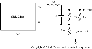 Figure 11. Reduced Ripple Configuration
8.2.2.2.2 Minimum Ripple Configuration
If the application requires a lower value of ripple (<10 mVp–p), the circuit of Figure 12 can be used. R3 is removed, and the resulting output ripple voltage is determined by the inductor’s ripple current and C2’s characteristics. RA and CA are chosen to generate a sawtooth waveform at their junction, and that voltage is AC-coupled to the FB pin through CB. To determine the values for RA, CA and CB, use Equation 10.
where
- VSW is the absolute value of the voltage at the SW pin during the off-time (typically 1 V)
VA is the DC voltage at the RA/CA junction, and is used in Equation 11.
where
- tON is the maximum on-time (at minimum input voltage)
- ΔV is the desired ripple amplitude at the RA/CA junction (typically 40 mV to 50 mV)
RA and CA are then chosen from standard value components to satisfy the above product. Typically CA is 1000 pF to 5000 pF, and RA is 10 kΩ to 300 kΩ. CB is then chosen large compared to CA, typically 0.1 µF.
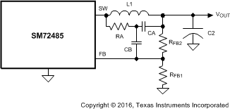 Figure 12. Minimum Output Ripple Using Ripple Injection
8.2.2.2.3 Alternate Minimum Ripple Configuration
The circuit in Figure 13 is the same as that in the block diagram, except the output voltage is taken from the junction of R3 and C2. The ripple at VOUT is determined by the inductor’s ripple current and C2’s characteristics. However, R3 slightly degrades the load regulation. This circuit may be suitable if the load current is fairly constant.
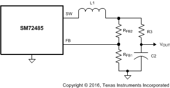 Figure 13. Alternate Minimum Output Ripple
8.2.3 Application Curves
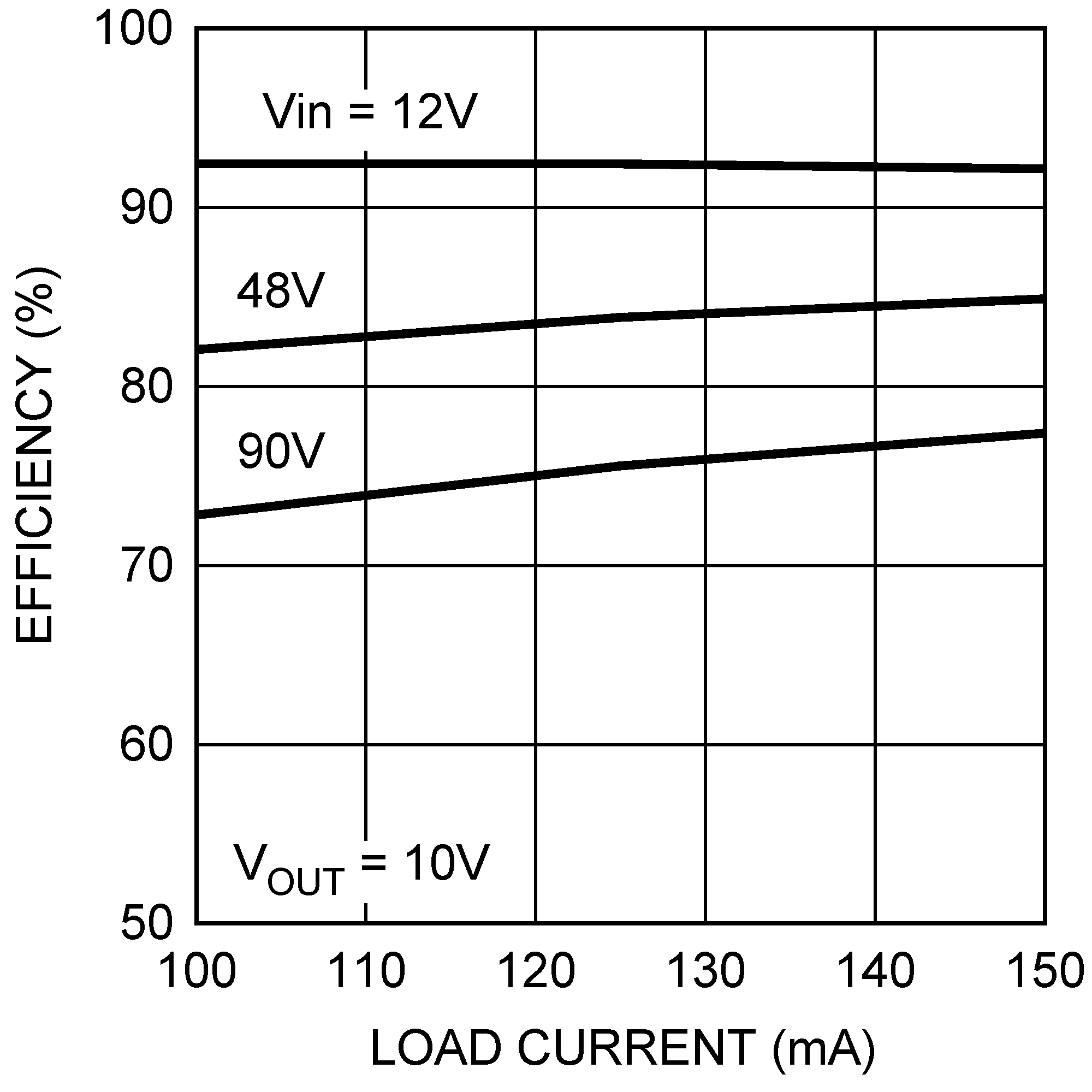 Figure 14. Efficiency vs Load Current and VIN
 Figure 15. Efficiency vs VIN