SNVS697E January 2011 – December 2016 SM72485
PRODUCTION DATA.
- 1 Features
- 2 Applications
- 3 Description
- 4 Revision History
- 5 Pin Configuration and Functions
- 6 Specifications
- 7 Detailed Description
- 8 Application and Implementation
- 9 Power Supply Recommendations
- 10Layout
- 11Device and Documentation Support
- 12Mechanical, Packaging, and Orderable Information
10 Layout
10.1 Layout Guidelines
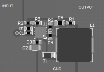
A proper layout is essential for optimum performance of the circuit. In particular, the following guidelines must be observed.
- CIN: The loop consisting of input capacitor (CIN), VIN pin, and RTN pin carries switching currents. Therefore, the input capacitor must be placed close to the IC, directly across VIN and RTN pins and the connections to these two pins must be direct to minimize the loop area. In general, it is not possible to accommodate all of input capacitance near the IC. A good practice is to use a 0.1-µF or 0.47-µF capacitor directly across the VIN and RTN pins close to the IC, and the remaining bulk capacitor as close as possible.
- CVCC and CBST: The VCC and bootstrap (BST) bypass capacitors supply switching currents to the high- and low-side gate drivers. These two capacitors must also be placed as close to the IC as possible, and the connecting trace length and loop area must be minimized.
- The Feedback trace carries the output voltage information and a small ripple component that is necessary for proper operation of SM72485. Therefore, take care while routing the feedback trace to avoid coupling any noise to this pin. In particular, feedback trace must not run close to magnetic components, or parallel to any other switching trace.
- SW trace: The SW node switches rapidly between VIN and GND every cycle and is therefore a possible source of noise. The SW node area must be minimized. In particular, the SW node must not be inadvertently connected to a copper plane or pour.
10.2 Layout Example
 Figure 16. Layout Recommendation