SNVS697E January 2011 – December 2016 SM72485
PRODUCTION DATA.
- 1 Features
- 2 Applications
- 3 Description
- 4 Revision History
- 5 Pin Configuration and Functions
- 6 Specifications
- 7 Detailed Description
- 8 Application and Implementation
- 9 Power Supply Recommendations
- 10Layout
- 11Device and Documentation Support
- 12Mechanical, Packaging, and Orderable Information
5 Pin Configuration and Functions
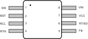
DGK Package
8-Pin VSSOP
Top View

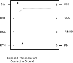
NGU Package
8-Pin WSON
Top View

Pin Functions
| PIN | TYPE(1) | DESCRIPTION | ||
|---|---|---|---|---|
| NAME | VSSOP | WSON | ||
| BST | 2 | 2 | I | An external capacitor is required between the BST and the SW pins. TI recommends a 0.01-µF ceramic capacitor. An internal diode charges the capacitor from VCC during each off-time. |
| FB | 5 | 5 | I | This pin is connected to the inverting input of the internal regulation comparator. The regulation threshold is 2.5 V. |
| RCL | 3 | 3 | I | A resistor between this pin and RTN sets the off-time when current limit is detected. The off-time is preset to 35 µs if FB = 0 V. |
| RT/SD | 6 | 6 | I | A resistor between this pin and VIN sets the switch on-time as a function of VIN. The minimum recommended on-time is 400 ns at the maximum input voltage. This pin can be used for remote shutdown. |
| RTN | 4 | 4 | G | Ground for the entire circuit. |
| SW | 1 | 1 | O | Power switching node. Connect to the output inductor, re-circulating diode, and bootstrap capacitor. |
| VCC | 7 | 7 | I | This regulated voltage provides gate drive power for the internal Buck switch. An internal diode is provided between this pin and the BST pin. A local 0.47-µF decoupling capacitor is required. The series pass regulator is current limited to 9 mA. |
| VIN | 8 | 8 | I | Input operating voltage: 6 V to 95 V. |
| Exposed Pad | — | Thermal Pad | NC | The exposed pad has no electrical contact. Connect to system ground plane for reduced thermal resistance. |
(1) G = Ground, I = Input, O = Output, NC = No Contact