ZHCSDS0B July 2011 – May 2015 SM74101
PRODUCTION DATA.
7 Detailed Description
7.1 Overview
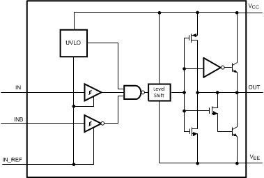
The SM74101 is a high speed, high peak current (7A) single channel MOSFET driver. The high peak output current of the SM74101 will switch power MOSFET’s on and off with short rise and fall times, thereby reducing switching losses considerably. The SM74101 includes both inverting and non-inverting inputs that give the user flexibility to drive the MOSFET with either active low or active high logic signals. The driver output stage consists of a compound structure with MOS and bipolar transistor operating in parallel to optimize current capability over a wide output voltage and operating temperature range. The bipolar device provides high peak current at the critical Miller plateau region of the MOSFET VGS , while the MOS device provides rail-to-rail output swing. The totem pole output drives the MOSFET gate between the gate drive supply voltage VCC and the power ground potential at the VEE pin.
7.2 Functional Block Diagram

7.3 Feature Description
7.3.1 Detailed Operating Description
The control inputs of the driver are high impedance CMOS buffers with TTL compatible threshold voltages. The negative supply of the input buffer is connected to the input ground pin IN_REF. An internal level shifting circuit connects the logic input buffers to the totem pole output drivers. The level shift circuit and the separate input/output ground pins provide the option of single supply or split supply configurations. When driving the MOSFET gate from a single positive supply, the IN_REF and VEE pins are both connected to the power ground.
The isolated input and output stage grounds provide the capability to drive the MOSFET to a negative VGS voltage for a more robust and reliable off state. In split supply configuration, the IN_REF pin is connected to the ground of the controller which drives the SM74101 inputs. The VEE pin is connected to a negative bias supply that can range from the IN_REF potential to as low as 14 V below the Vcc gate drive supply. For reliable operation, the maximum voltage difference between VCC and IN_REF or between VCC and VEE is 14V.
The minimum recommended operating voltage between Vcc and IN_REF is 3.5V. An Under Voltage Lock Out (UVLO) circuit is included in the SM74101 which senses the voltage difference between VCC and the input ground pin, IN_REF. When the VCC to IN_REF voltage difference falls below 2.8V the driver is disabled and the output pin is held in the low state. The UVLO hysteresis prevents chattering during brown-out conditions; the driver will resume normal operation when the VCC to IN_REF differential voltage exceeds 3.0V.
7.4 Device Functional Modes
7.4.1 Inverting Mode of Operation
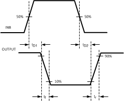
During the inverting mode of operation, INB is used as the control input and the polarity of OUT is reversed with respect to INB. A timing diagram of this mode is shown in Figure 11. The IN pin is not used in this mode of operation and should be pulled up to VCC.

7.4.2 Non-inverting Mode of Operation
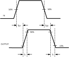
During the non-inverting mode of operation, IN is used as the control input and the polarity of OUT is the same with respect to IN. A timing diagram of this mode is shown in Figure 12. The INB pin is not used in this mode of operation and should be connected to IN_REF.

7.5 Thermal Considerations
The primary goal of the thermal management is to maintain the integrated circuit (IC) junction temperature (Tj) below a specified limit to ensure reliable long term operation. The maximum TJ of IC components should be estimated in worst case operating conditions. The junction temperature can be calculated based on the power dissipated on the IC and the junction to ambient thermal resistance θJA for the IC package in the application board and environment. The θJA is not a given constant for the package and depends on the PCB design and the operating environment.
7.5.1 Drive Power Requirement Calculations In SM74101
SM74101 is a single low side MOSFET driver capable of sourcing / sinking 3A / 7A peak currents for short intervals to drive a MOSFET without exceeding package power dissipation limits. High peak currents are required to switch the MOSFET gate very quickly for operation at high frequencies.
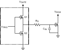
 Figure 13.
The schematic above shows a conceptual diagram of the SM74101 output and MOSFET load. Q1 and Q2 are the switches within the gate driver. Rg is the gate resistance of the external MOSFET, and Cin is the equivalent gate capacitance of the MOSFET. The equivalent gate capacitance is a difficult parameter to measure as it is the combination of Cgs (gate to source capacitance) and Cgd (gate to drain capacitance). The Cgd is not a constant and varies with the drain voltage. The better way of quantifying gate capacitance is the gate charge Qg in coloumbs. Qg combines the charge required by Cgs and Cgd for a given gate drive voltage Vgate. The gate resistance Rg is usually very small and losses in it can be neglected. The total power dissipated in the MOSFET driver due to gate charge is approximated by:
where
- FSW = switching frequency of the MOSFET.
For example, consider the MOSFET MTD6N15 whose gate charge specified as 30 nC for VGATE = 12V.
Therefore, the power dissipation in the driver due to charging and discharging of MOSFET gate capacitances at switching frequency of 300 kHz and VGATE of 12V is equal to
In addition to the above gate charge power dissipation, - transient power is dissipated in the driver during output transitions. When either output of the SM74101 changes state, current will flow from VCC to VEE for a very brief interval of time through the output totem-pole N and P channel MOSFETs. The final component of power dissipation in the driver is the power associated with the quiescent bias current consumed by the driver input stage and Under-voltage lockout sections.
Characterization of the SM74101 provides accurate estimates of the transient and quiescent power dissipation components. At 300 kHz switching frequency and 30 nC load used in the example, the transient power will be 8 mW. The 1 mA nominal quiescent current and 12V VGATE supply produce a 12 mW typical quiescent power.
Therefore the total power dissipation
We know that the junction temperature is given by
Or the rise in temperature is given by
For WSON-6 package, the integrated circuit die is attached to leadframe die pad which is soldered directly to the printed circuit board. This substantially decreases the junction to ambient thermal resistance (θJA). By providing suitable means of heat dispersion from the IC to the ambient through exposed copper pad, which can readily dissipate heat to the surroundings, θJA as low as 40°C / Watt is achievable with the package. The resulting Trise for the driver example above is thereby reduced to just 5.5 degrees.
Therefore TRISE is equal to