ZHCSRN0F July 1995 – November 2024 SN54ACT04 , SN74ACT04
PRODUCTION DATA
- 1
- 1 特性
- 2 应用
- 3 说明
- 4 Pin Configuration and Functions
- 5 Specifications
- 6 Parameter Measurement Information
- 7 Detailed Description
- 8 应用信息免责声明
- 9 Device and Documentation Support
- 10Revision History
- 11Mechanical, Packaging, and Orderable Information
封装选项
请参考 PDF 数据表获取器件具体的封装图。
机械数据 (封装 | 引脚)
- J|14
- FK|20
- W|14
散热焊盘机械数据 (封装 | 引脚)
订购信息
4 Pin Configuration and Functions
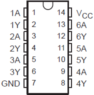
 Figure 4-1 SN54ACT04 J or W Package;
SN74ACT04 D, DB, N, NS, or PW Package (Top View)
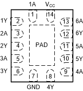
 Figure 4-2 BQA Package, 14-Pin WQFN (Top View)
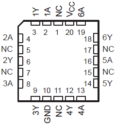
 Figure 4-3 SN54ACT04 FK Package (Top View)
Table 4-1 Pin Functions
| PIN | I/O(1) | DESCRIPTION | ||
|---|---|---|---|---|
| NAME | BQA, D, DB, N, NS, PW, J, or W | FK | ||
| 1A | 1 | 2 | Input | Channel 1, Input A |
| 1Y | 2 | 3 | Output | Channel 1, Output Y |
| 2A | 3 | 4 | Input | Channel 2, Input A |
| 2Y | 4 | 6 | Output | Channel 2, Output Y |
| 3A | 5 | 8 | Input | Channel 3, Input A |
| 3Y | 6 | 9 | Output | Channel 3, Output Y |
| GND | 7 | 10 | — | Ground |
| 4Y | 8 | 12 | Output | Channel 4, Output Y |
| 4A | 9 | 13 | Input | Channel 4, Input A |
| 5Y | 10 | 14 | Output | Channel 5, Output Y |
| 5A | 11 | 16 | Input | Channel 5, Input A |
| 6Y | 12 | 18 | Output | Channel 6, Output Y |
| 6A | 13 | 19 | Input | Channel 6, Input A |
| VCC | 14 | 20 | — | Positive Supply |
| NC | 1, 5, 7, 11, 15, 17 | — | Not internally connected | |
| Thermal pad | — | Connect the GND pin to the exposed thermal pad for correct operation. Connect the thermal pad to any internal PCB ground plane using multiple vias for good thermal performance. | ||
(1) I = input, O = output, P =
power, FB = feedback, GND = ground, N/A = not applicable