ZHCSNA8H December 1982 – August 2021 SN54HC00 , SN74HC00
PRODUCTION DATA
- 1 特性
- 2 应用
- 3 说明
- 4 Revision History
- 5 Pin Configuration and Functions
-
6 Specifications
- 6.1 Absolute Maximum Ratings
- 6.2 ESD Ratings
- 6.3 Recommended Operating Conditions
- 6.4 Thermal Information
- 6.5 Electrical Characteristics - Commercial (74xx)
- 6.6 Electrical Characteristics - Military (54xx)
- 6.7 Switching Characteristics - Commercial (74xx)
- 6.8 Switching Characteristics - Military (54xx)
- 6.9 Typical Characteristics
- 7 Parameter Measurement Information
- 8 Detailed Description
- 9 Application and Implementation
- 10Power Supply Recommendations
- 11Layout
- 12Device and Documentation Support
- 13Mechanical, Packaging, and Orderable Information
封装选项
机械数据 (封装 | 引脚)
散热焊盘机械数据 (封装 | 引脚)
订购信息
6.9 Typical Characteristics
TA = 25°C
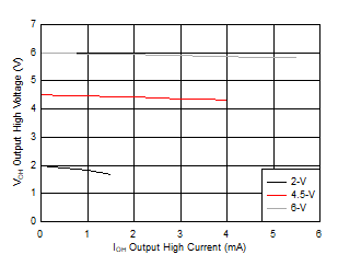
 Figure 6-1 Typical Output
Voltage in the High State (VOH)
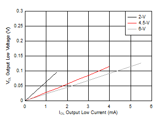
 Figure 6-2 Typical Output Voltage in
the Low State (VOL)