SCLS116H December 1982 – December 2015 SN54HC165 , SN74HC165
PRODUCTION DATA.
- 1 Features
- 2 Applications
- 3 Description
- 4 Revision History
- 5 Pin Configuration and Functions
-
6 Specifications
- 6.1 Absolute Maximum Ratings
- 6.2 ESD Ratings
- 6.3 Recommended Operating Conditions
- 6.4 Thermal Information
- 6.5 Electrical Characteristics, TA = 25°C
- 6.6 Electrical Characteristics, SN54HC165
- 6.7 Electrical Characteristics, SN74HC165
- 6.8 Switching Characteristics, TA = 25°C
- 6.9 Switching Characteristics, SN54HC165
- 6.10 Switching Characteristics, SN74HC165
- 6.11 Timing Requirements, TA = 25°C
- 6.12 Timing Requirements, SN54HC165
- 6.13 Timing Requirements, SN74HC165
- 6.14 Operating Characteristics
- 6.15 Typical Characteristics
- 7 Parameter Measurement Information
- 8 Detailed Description
- 9 Application and Implementation
- 10Power Supply Recommendations
- 11Layout
- 12Device and Documentation Support
- 13Mechanical, Packaging, and Orderable Information
封装选项
请参考 PDF 数据表获取器件具体的封装图。
机械数据 (封装 | 引脚)
- W|16
- J|16
- FK|20
散热焊盘机械数据 (封装 | 引脚)
订购信息
8 Detailed Description
8.1 Overview
The SNx4HC165 is an 8-bit Parallel load shift register with 1 serial input and 8 parallel load input. The device loads all the 8 bits simultaneously through parallel load input when SH/LD is low. This will also ignore any input at CLK or CLK INH.
The device shifts the data when CLK toggles. The data is shifted on rising edge of the clock. Clock Inhibit (CLK INH) inhibits the clock function resulting in no change of the output. If SH/LD is low clock inputs are ignored. To realize the shift function, SH/LD should be high.
CLK and CLK INH functions are interchangeable. If CLK is low then change a clock signal at CLK INH pin causes a shift of data to QH. If CLK INH is Low clock signal on CLK pin shifts the data out to QH.
8.2 Functional Block Diagram
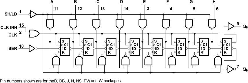
 Figure 3. Logic Diagram Positive Logic
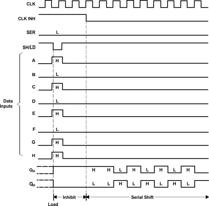
 Figure 4. Typical Shift, Load, and Inhibit Sequence
8.3 Feature Description
The SNx4HC165 has a wide operating voltage range of 2 V to 6 V, outputs that can drive up to 10 LSTTL loads and Low Power Consumption, 80-μA maximum I. It is typically tpd = 13 ns and has ±4-mA output drive at 5 V with low input current of 1-μA maximum. The device features the direct overloading load of data input, meaning parallel data is loaded irrespective of clock signals.
8.4 Device Functional Table
Table 1 lists the functional modes of the SNx4HC165.