ZHCSPJ9B February 2022 – December 2023 SN54SLC8T245-SEP
PRODUCTION DATA
- 1
- 1 特性
- 2 应用
- 3 说明
- 4 Pin Configuration and Functions
-
5 Specifications
- 5.1 Absolute Maximum Ratings
- 5.2 ESD Ratings
- 5.3 Recommended Operating Conditions
- 5.4 Thermal Information
- 5.5 Electrical Characteristics
- 5.6 Switching Characteristics, VCCA = 0.7 V
- 5.7 Switching Characteristics, VCCA = 0.8 V
- 5.8 Switching Characteristics, VCCA = 0.9 V
- 5.9 Switching Characteristics, VCCA = 1.2 V
- 5.10 Switching Characteristics, VCCA = 1.5 V
- 5.11 Switching Characteristics, VCCA = 1.8 V
- 5.12 Switching Characteristics, VCCA = 2.5 V
- 5.13 Switching Characteristics, VCCA = 3.3 V
- 5.14 Operating Characteristics
- 6 Parameter Measurement Information
- 7 Detailed Description
- 8 Application and Implementation
- 9 Device and Documentation Support
- 10Revision History
- 11Mechanical, Packaging, and Orderable Information
6 Parameter Measurement Information
Unless otherwise noted, all input pulses are supplied by generators having the following characteristics:
- f =1 MHz
- Z0 = 50 Ω
- dv / dt ≤ 1 ns/V

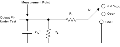
A. CL
includes probe and jig capacitance.
Figure 6-1 Load
Circuit
A. Output waveform on
the conditions that input is driven to a valid Logic Low.
B. Output waveform on
the condition that input is driven to a valid Logic High.
Figure 6-2 Load
Circuit Conditions
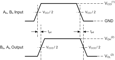
A. VCCI is the
supply pin associated with the input port.
B. VOH and
VOL are typical output voltage levels with specified
RL, CL, and S1.
Figure 6-3 Propagation Delay
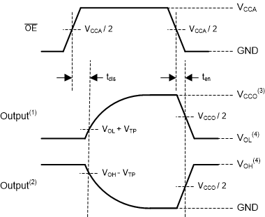
A. Output waveform
on the condition that input is driven to a valid Logic Low.
B. Output waveform
on the condition that input is driven to a valid Logic High.
C. VCCO is
the supply pin associated with the output port.
D. VOH and
VOL are typical output voltage levels with specified
RL, CL, and S1.
Figure 6-4 Enable Time And Disable Time