SLLS545G November 2002 – October 2015 SN55HVD251 , SN65HVD251
PRODUCTION DATA.
- 1 Features
- 2 Applications
- 3 Description
- 4 Revision History
- 5 Pin Configuration and Functions
-
6 Specifications
- 6.1 Absolute Maximum Ratings
- 6.2 ESD Ratings
- 6.3 Recommended Operating Conditions
- 6.4 Thermal Information
- 6.5 Supply Current
- 6.6 Electrical Characteristics: Driver
- 6.7 Electrical Characteristics: Receiver
- 6.8 VREF-Pin Characteristics
- 6.9 Power Dissipation Characteristics
- 6.10 Switching Characteristics: Driver
- 6.11 Switching Characteristics: Device
- 6.12 Switching Characteristics: Receiver
- 6.13 Dissipation Ratings
- 6.14 Typical Characteristics
- 7 Parameter Measurement Information
- 8 Detailed Description
- 9 Application and Implementation
- 10Power Supply Recommendations
- 11Layout
- 12Device and Documentation Support
- 13Mechanical, Packaging, and Orderable Information
8 Detailed Description
8.1 Overview
The SNx5HVD251CAN bus transceiver is compatible with the ISO 11898-2 High Speed CAN (Controller Area Network) physical layer standard. It is design to interface between the differential bus lines in controller area network and the CAN protocol controller at data rates up to 1 Mbps.
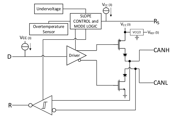
8.2 Functional Block Diagram

8.3 Feature Description
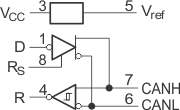
 Figure 23. Function Diagram (Positive Logic)
8.3.1 Mode Control
RS, Pin 8, selects one of three possible modes of operation: high-speed, slope control, or low-power mode.
8.3.2 High-Speed Mode
The high-speed mode of operation can be selected by setting RS (Pin 8) low. High-speed allows the output to switch as fast as possible with no internal limitations on the output rise and fall slopes. The CAN bus driver and receiver are fully operational and the CAN communication is bi-directional. The driver is translating a digital input on D to a differential output on CANH and CANL. The receiver is translating the differential signal from CANH and CANL to a digital output on R.
8.3.3 Slope Control Mode
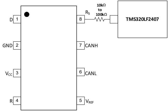
The rise and fall slope of the SNx5HVD251 driver output can be adjusted by connecting a resistor from Rs (Pin 8) to ground (GND), or to a low-level input voltage as shown in Figure 24. The slope of the driver output signal is proportional to the pin's output current. This slope control is implemented with an external resistor value of 10 kΩ to achieve a ~15-V/μs slew rate, and up to 100 kΩ to achieve a ~2.0-V/μs slew rate. Figure 8 shows a plot of differential output transition time vs slope resistance from which the slew rate can be calculated.
8.3.4 Low-Power Mode
If a high-level input (>0.75 VCC) is applied to RS (Pin 8), the circuit enters a low-current, listen only standby mode during which the driver is switched off and the receiver remains active. If using this mode to save system power while waiting for bus traffic, the local controller can monitor the R output pin for a falling edge which indicates that a dominant signal was driven onto the CAN bus. The local controller can then drive the RS pin low to return to slope control mode or high-speed mode.
NOTE
Silent mode may be used to implement babbling idiot protection, to ensure that the driver does not disrupt the network during a local fault. Silent mode may also be used in redundant systems to select or de-select the redundant transceiver (driver) when needed.
 Figure 24. Slope Control
8.3.5 Thermal Shutdown
The SNx5HVD251 has a thermal shutdown feature that turns off the driver outputs when the junction temperature nears 165°C. This shutdown prevents catastrophic failure from bus shorts, but does not protect the circuit from possible damage. The user should strive to maintain recommended operating conditions and not exceed absolute-maximum ratings at all times. If an SNx5HVD251 is subjected to many, or long-duration faults that can put the device into thermal shutdown, it should be replaced.
8.4 Device Functional Modes
Table 2. Driver
| INPUTS | Voltage at Rs, VRs | OUTPUTS | BUS STATE | |
|---|---|---|---|---|
| D | CANH | CANL | ||
| L | VRs < 1.2 V | H | L | Dominant |
| H | VRs < 1.2 V | Z | Z | Recessive |
| Open | X | Z | Z | Recessive |
| X | VRs > 0.75 VCC | Z | Z | Recessive |
| X | Open | Z | Z | Recessive |
Table 3. Receiver
| DIFFERENTIAL INPUTS [VID = V(CANH) - V(CANL)] | OUTPUT R(1) |
|---|---|
| VID ≥ 0.9 V | L |
| 0.5 V < VID < 0.9 V | ? |
| VID ≤ 0.5 V | H |
| Open | H |
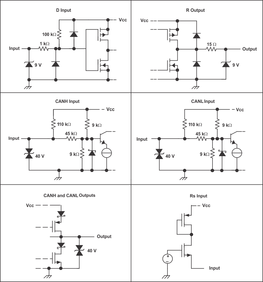
 Figure 25. Equivalent Input and Output Schematic Diagrams