ZHCSE84A October 2015 – February 2017 SN55HVD75-EP
PRODUCTION DATA.
9 Application and Implementation
NOTE
Information in the following applications sections is not part of the TI component specification, and TI does not warrant its accuracy or completeness. TI’s customers are responsible for determining suitability of components for their purposes. Customers should validate and test their design implementation to confirm system functionality.
9.1 Application Information
The SN55HVD75-EP is a half-duplex RS-485 transceiver commonly used for asynchronous data transmission. The driver and receiver enable pins allow for the configuration of different operating modes.
 Figure 15. Transceiver Configurations
Using independent enable lines provides the most flexible control as it allows for the driver and the receiver to be turned on and off individually. While this configuration requires two control lines, it allows for selective listening into the bus traffic, whether the driver is transmitting data or not.
Combining the enable signals simplifies the interface to the controller by forming a single direction-control signal. In this configuration, the transceiver operates as a driver when the direction-control line is high, and as a receiver when the direction-control line is low.
Additionally, only one line is required when connecting the receiver-enable input to ground and controlling only the driver-enable input. In this configuration, a node not only receives the data from the bus, but also the data it sends and can verify that the correct data have been transmitted.
9.2 Typical Application
An RS-485 bus consists of multiple transceivers connected in parallel to a bus cable. To eliminate line reflections, each cable end is terminated with a termination resistor, RT, whose value matches the characteristic impedance, Z0, of the cable. This method, known as parallel termination, allows for relatively high data rates over long cable lengths.
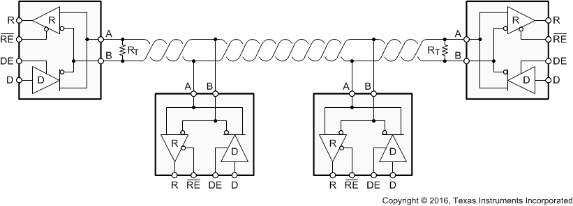 Figure 16. Typical RS-485 Network With SN55HVD75-EP Transceivers
Common cables used are unshielded twisted pair (UTP), such as low-cost CAT-5 cable with Z0 = 100 Ω, and
RS-485 cable with Z0 = 120 Ω. Typical cable sizes are AWG 22 and AWG 24.
The maximum bus length is typically given as 4000 ft or 1200 m, and represents the length of an AWG 24 cable whose cable resistance approaches the value of the termination resistance, thus reducing the bus signal by half or 6 dB. Actual maximum usable cable length depends on the signaling rate, cable characteristics, and environmental conditions.
9.2.1 Design Requirements
RS-485 is a robust electrical standard suitable for long-distance networking that may be used in a wide range of applications with varying requirements, such as distance, data rate, and number of nodes.
9.2.1.1 Data Rate and Bus Length
There is an inverse relationship between data rate and bus length, meaning the higher the data rate, the shorter the cable length; and conversely, the lower the data rate, the longer the cable may be without introducing data errors. While most RS-485 systems use data rates between 10 kbps and 100 kbps, some applications require data rates up to 250 kbps at distances of 4000 feet and longer. Longer distances are possible by allowing for small signal jitter of up to 5 or 10%.
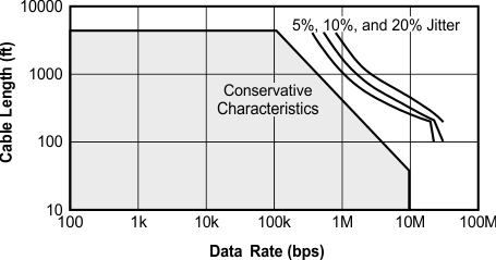 Figure 17. Cable Length vs Data Rate Characteristic
9.2.1.2 Stub Length
When connecting a node to the bus, the distance between the transceiver inputs and the cable trunk, known as the stub, should be as short as possible. Stubs present a non-terminated piece of bus line which can introduce reflections as the length of the stub increases. As a general guideline, the electrical length, or round-trip delay, of a stub should be less than one-tenth of the rise time of the driver, thus giving a maximum physical stub length as shown in Equation 1.
where
- tr is the 10/90 rise time of the driver
- c is the speed of light (3 × 10⁸ m/s)
- v is the signal velocity of the cable or trace as a factor of c
Per Equation 1, Table 3 shows the maximum cable-stub lengths for the minimum driver output rise times of the SN55HVD75-EP half-duplex transceiver for a signal velocity of 78%.
Table 3. Maximum Stub Length
| DEVICE | MINIMUM DRIVER OUTPUT RISE TIME (ns) |
MAXIMUM STUB LENGTH | |
|---|---|---|---|
| (m) | (ft) | ||
| SN55HVD75-EP | 2 | 0.05 | 0.16 |
9.2.1.3 Bus Loading
The RS-485 standard specifies that a compliant driver must be able to drive 32 unit loads (UL), where 1 unit load represents a receiver input current of 1 mA at 12 V, or a load impedance of approximately 12 kΩ. Because the SN55HVD75-EP has a receiver input current of 150 µA at 12 V, they are 3/20 UL transceivers, and no more than 213 transceivers should be connected to the bus.
9.2.1.4 Receiver Failsafe
The differential receiver is failsafe to invalid bus states caused by:
- Open bus conditions such as a disconnected connector
- Shorted bus conditions such as cable damage shorting the twisted-pair together, or
- Idle bus conditions that occur when no driver on the bus is actively driving
Receiver failsafe is accomplished by offsetting the receiver thresholds such that the input-indeterminate range does not include 0-V differential. To comply with RS-485 standards, the receiver output must output a high when the differential input VID is more positive than 200 mV, and must output a low when VID is more negative than –200 mV. The receiver parameters which determine the failsafe performance are VIT+, VIT–, and VHYS (the separation between VIT+ and VIT–). As shown in Electrical Characteristics, differential signals more negative than –200 mV will always cause a low receiver output, and differential signals more positive than 200 mV will always cause a high receiver output.
When the differential input signal is close to zero, it is still above the maximum VIT+ threshold of –20 mV, and the receiver output will be high. Only when the differential input is more than VHYS below VIT+ will the receiver output transition to a low state. Therefore, the noise immunity of the receiver inputs during a bus fault condition includes the receiver hysteresis value, VHYS, as well as the value of VIT+.
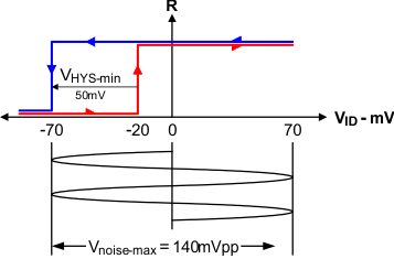 Figure 18. Noise Immunity
9.2.1.5 Transient Protection
The bus pins of the SN55HVD75-EP transceiver family possess on-chip ESD protection against ±15-kV human body model (HBM) and ±12-kV IEC 61000-4-2 contact discharge. The IEC-ESD test is far more severe than the HBM-ESD test. The 50% higher charge capacitance, CS, and 78% lower discharge resistance, RD, of the IEC-model produce significantly higher discharge currents than the HBM-model.
As stated in the IEC 61000-4-2 standard, contact discharge is the preferred test method; although IEC air-gap testing is less repeatable than contact testing, air discharge protection levels are inferred from the contact discharge test results.
 Figure 19. HBM and IEC-ESD Models and Currents in Comparison (HBM Values in Parenthesis)
The on-chip implementation of IEC ESD protection significantly increases the robustness of equipment. Common discharge events occur due to human contact with connectors and cables. Designers may choose to implement protection against longer duration transients, typically referred to as surge transients.
EFTs are generally caused by relay-contact bounce or the interruption of inductive loads. Surge transients often result from lightning strikes (direct strike or an indirect strike which induce voltages and currents), or the switching of power systems, including load changes and short circuit switching. These transients are often encountered in industrial environments, such as factory automation and power-grid systems.
Figure 20 compares the pulse-power of the EFT and surge transients with the power caused by an IEC ESD transient. The left-hand diagram shows the relative pulse-power for a 0.5-kV surge transient and 4-kV EFT transient, both of which dwarf the 10-kV ESD transient visible in the lower-left corner. 500-V surge transients are representative of events that may occur in factory environments in industrial and process automation.
The right-hand diagram shows the pulse-power of a 6-kV surge transient, relative to the same 0.5-kV surge transient. 6-kV surge transients are most likely to occur in power generation and power-grid systems.
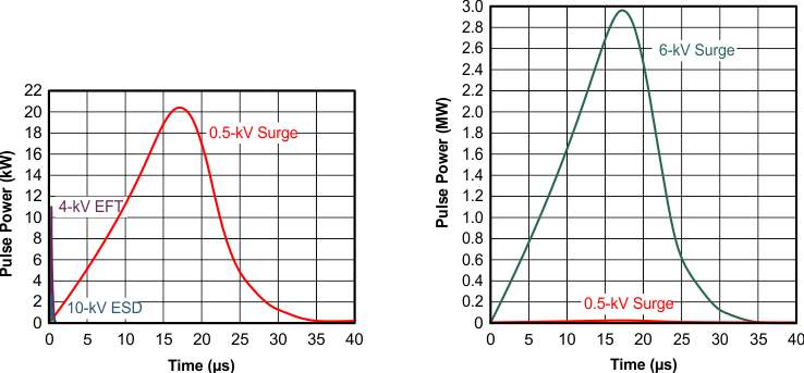 Figure 20. Power Comparison of ESD, EFT, and Surge Transients
In the case of surge transients, high-energy content is characterized by long pulse duration and slow decaying pulse power. The electrical energy of a transient that is dumped into the internal protection cells of a transceiver is converted into thermal energy which heats and destroys the protection cells, thus destroying the transceiver. Figure 21 shows the large differences in transient energies for single ESD, EFT, and surge transients, as well as for an EFT pulse train, commonly applied during compliance testing.
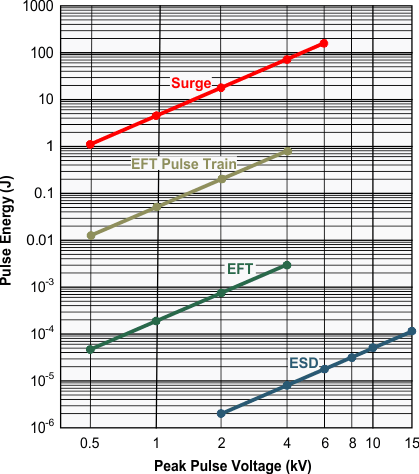 Figure 21. Comparison of Transient Energies
9.2.2 Detailed Design Procedure
9.2.2.1 External Transient Protection
To protect bus nodes against high-energy transients, the implementation of external transient protection devices is necessary. Figure 22 suggests two circuits that provide protection against light and heavy surge transients, in addition to ESD and EFT transients. Table 4 presents the associated bill of materials.
Table 4. Bill of Materials
| DEVICE | FUNCTION | ORDER NUMBER | MANUFACTURER |
|---|---|---|---|
| XCVR | 3.3-V, 250-kbps RS-485 transceiver | SN55HVD75DRBREP | TI |
| R1, R2 | 10-Ω, pulse-proof thick-film resistor | CRCW060310RJNEAHP | Vishay |
| TVS | Bidirectional 400-W transient suppressor | CDSOT23-SM712 | Bourns |
| TBU1, TBU2 | Bidirectional surge suppressor | TBU-CA-065-200-WH | Bourns |
| MOV1, MOV2 | 200-mA Transient blocking unit, 200-V, metal-oxide varistor | MOV-10D201K | Bourns |
 Figure 22. Transient Protections against ESD, EFT, and Surge Transients
The left-hand circuit provides surge protection of ≥500-V surge transients, while the right-hand circuit can withstand surge transients of up to 5 kV.
9.2.2.2 Isolated Bus Node Design
Many RS-485 networks use isolated bus nodes to prevent the creation of unintended ground loops and their disruptive impact on signal integrity. An isolated bus node typically includes a microcontroller that connects to the bus transceiver via a multi-channel, digital isolator (Figure 23).
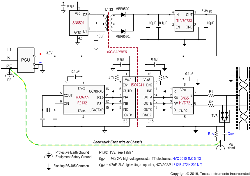 Figure 23. Isolated Bus Node with Transient Protection
Power isolation is accomplished using the push-pull transformer driver SN6501 and a low-cost LDO, TLV70733.
Signal isolation uses the quadruple digital isolator ISO7241. Notice that both enable inputs, EN1 and EN2, are pulled up via 4.7-kΩ resistors to limit their input currents during transient events.
While the transient protection is similar to the one in Figure 22 (left circuit), an additional high-voltage capacitor is used to divert transient energy from the floating RS-485 common further toward Protective Earth (PE) ground. This is necessary as noise transients on the bus are usually referred to Earth potential.
RHV refers to a high voltage resistor, and in some applications even a varistor. This resistance is applied to prevent charging of the floating ground to dangerous potentials during normal operation.
Occasionally varistors are used instead of resistors to rapidly discharge CHV, if it is expected that fast transients might charge CHV to high-potentials.
Note that the PE island represents a copper island on the PCB for the provision of a short, thick Earth wire connecting this island to PE ground at the entrance of the power supply unit (PSU).
In equipment designs using a chassis, the PE connection is usually provided through the chassis itself. Typically the PE conductor is tied to the chassis at one end while the high-voltage components, CHV and RHV, are connecting to the chassis at the other end.
9.2.3 Application Curve
| RL = 60 Ω |