ZHCSLK2 September 2020 SN55LVCP22
PRODUCTION DATA
- 1 特性
- 2 应用
- 3 说明
- 4 Revision History
- 5 Pin Configuration and Functions
- 6 Specifications
- 7 Parameter Measurement Information
- 8 Detailed Description
- 9 Application and Implementation
- 10Power Supply Recommendations
- 11Layout
- 12Device and Documentation Support
- 13Mechanical, Packaging, and Orderable Information
7 Parameter Measurement Information
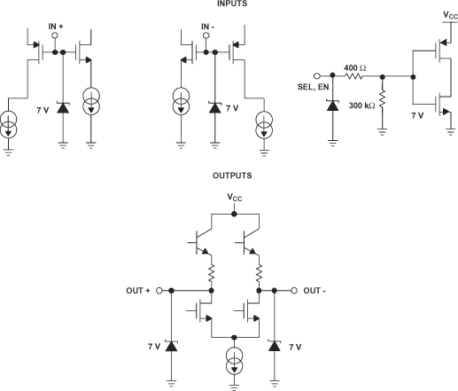
 Figure 7-1 Equivalent Input and Output Schematic Diagrams
 Figure 7-2 Voltage
And Current Definitions
 Figure 7-3 Differential Output Voltage (VOD) Test Circuit
All input
pulses are supplied by a generator having the following characteristics:
tr or tf ≤ 1 ns, pulse-repetition rate (PRR) = 0.5
Mpps, pulse width = 500 ±10 ns; RL = 100 Ω; CL includes
instrumentation and fixture capacitance within 0,06 mm of the D.U.T.; the
measurement of VOC(PP) is made on test equipment with a –3 dB
bandwidth of at least 300 MHz.
Figure 7-4 Test
Circuit And Definitions For The Driver Common-Mode Output Voltage
All input
pulses are supplied by a generator having the following characteristics:
tr or tf ≤ .25 ns, pulse-repetition rate (PRR) = 0.5
Mpps, pulse width = 500 ± 10 ns. CL includes instrumentation and
fixture capacitance within 0,06 mm of the D.U.T.
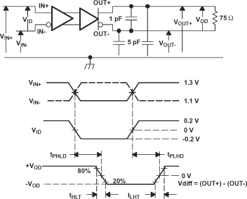
Figure 7-5 Timing
Test Circuit And Waveforms
All input
pulses are supplied by a generator having the following characteristics:
tr or tf ≤ 1 ns, pulse-repetition rate (PRR) = 0.5
Mpps, pulse width = 500 ± 10 ns. CL includes instrumentation and
fixture capacitance within 0,06 mm of the D.U.T.
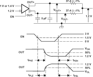
Figure 7-6 Enable
And Disable Time Circuit And DefinitionsTable 7-1 Receiver
Input Voltage Threshold Test
| APPLIED VOLTAGES | RESULTING DIFFERENTIAL INPUT VOLTAGE |
RESULTING COMMON- MODE INPUT VOLTAGE |
OUTPUT(1) | |
|---|---|---|---|---|
| VIA | VIB | VID | VIC | |
| 1.25 V | 1.15 V | 100 mV | 1.2 V | H |
| 1.15 V | 1.25 V | –100 mV | 1.2 V | L |
| 4.0 V | 3.9 V | 100 mV | 3.95 V | H |
| 3.9 V | 4. 0 V | –100 mV | 3.95 V | L |
| 0.1 V | 0.0 V | 100 mV | 0.05 V | H |
| 0.0 V | 0.1 V | –100 mV | 0.05 V | L |
| 1.7 V | 0.7 V | 1000 mV | 1.2 V | H |
| 0.7 V | 1.7 V | –1000 mV | 1.2 V | L |
| 4.0 V | 3.0 V | 1000 mV | 3.5 V | H |
| 3.0 V | 4.0 V | –1000 mV | 3.5 V | L |
| 1.0 V | 0.0 V | 1000 mV | 0.5 V | H |
| 0.0 V | 1.0 V | –1000 mV | 0.5 V | L |
(1) H = high level, L = low level

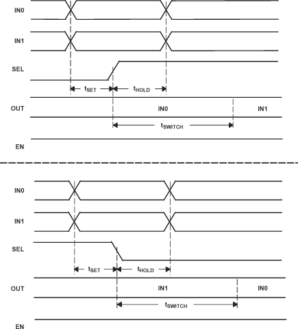
tSET
and tHOLD times specify that data must be in a stable state before
and after mux control switches.
Figure 7-7 Input To
Select For Both Rising And Falling Edge Setup And Hold Times