ZHCSB64C June   2013  – March 2021 SN6501-Q1

PRODUCTION DATA  

  1. 特性
  2. 应用
  3. 说明
  4. Revision History
  5. Pin Configuration and Functions
  6. Specifications
    1. 6.1 Absolute Maximum Ratings
    2. 6.2 Handling Ratings
    3. 6.3 Recommended Operating Conditions
    4. 6.4 Thermal Information
    5. 6.5 Electrical Characteristics
    6. 6.6 Switching Characteristics
    7. 6.7 Typical Characteristics
  7. Parameter Measurement Information
    1. 7.1 15
  8. Detailed Description
    1. 8.1 Overview
    2. 8.2 Functional Block Diagram
    3. 8.3 Feature Description
      1. 8.3.1 Push-Pull Converter
      2. 8.3.2 Core Magnetization
    4. 8.4 Device Functional Modes
      1. 8.4.1 Start-Up Mode
      2. 8.4.2 Operating Mode
      3. 8.4.3 Off-Mode
  9. Application and Implementation
    1. 9.1 Application Information
    2. 9.2 Typical Application
      1. 9.2.1 Design Requirements
      2. 9.2.2 Detailed Design Procedure
        1. 9.2.2.1 SN6501 Drive Capability
        2. 9.2.2.2 LDO Selection
        3. 9.2.2.3 Diode Selection
        4. 9.2.2.4 Capacitor Selection
        5. 9.2.2.5 Transformer Selection
          1. 9.2.2.5.1 V-t Product Calculation
          2. 9.2.2.5.2 Turns Ratio Estimate
          3. 9.2.2.5.3 Recommended Transformers
      3. 9.2.3 Application Curve
      4. 9.2.4 Higher Output Voltage Designs
      5. 9.2.5 Application Circuits
  10. 10Power Supply Recommendations
    1. 10.1 43
  11. 11Layout
    1. 11.1 Layout Guidelines
    2. 11.2 Layout Example
  12. 12Device and Documentation Support
    1. 12.1 Device Support
      1. 12.1.1 第三方米6体育平台手机版_好二三四免责声明
    2. 12.2 Trademarks
    3. 12.3 静电放电警告
    4. 12.4 术语表
  13. 13Mechanical, Packaging, and Orderable Information

封装选项

机械数据 (封装 | 引脚)
散热焊盘机械数据 (封装 | 引脚)
订购信息

Higher Output Voltage Designs

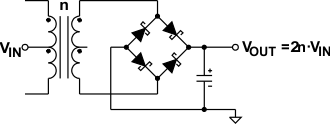
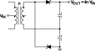
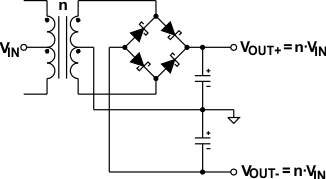
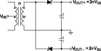
The SN6501 can drive push-pull converters that provide high output voltages of up to 30 V, or bipolar outputs of up to ±15 V. Using commercially available center-tapped transformers, with their rather low turns ratios of 0.8 to 5, requires different rectifier topologies to achieve high output voltages. #SLLSEA04407 to #SLLSEA0920 show some of these topologies together with their respective open-circuit output voltages.
GUID-DBFE9236-BD2F-4526-ADAA-83165E6A8AD7-low.gif
Figure 9-8 Bridge Rectifier With Center-Tapped Secondary Enables Bipolar Outputs
GUID-99B4A182-A317-40D6-832A-97B07119761A-low.gif
Figure 9-10 Half-Wave Rectifier Without Center-Tapped Secondary Performs Voltage Doubling, Centered Ground Provides Bipolar Outputs
GUID-AF9A1C16-2FF4-473B-BE6E-41497095916B-low.gif
Figure 9-9 Bridge Rectifier Without Center-Tapped Secondary Performs Voltage Doubling
GUID-FBA7B207-19EF-4913-98A3-1F92268A0F29-low.gif
Figure 9-11 Half-Wave Rectifier Without Centered Ground and Center-Tapped Secondary Performs Voltage Doubling Twice, Hence Quadrupling VIN