ZHCSUM3C March 2007 – February 2024 SN65C1167E , SN65C1168E
PRODUCTION DATA
- 1
- 1 特性
- 2 应用
- 3 说明
- 4 Pin Configuration and Functions
-
5 Specifications
- 5.1 Absolute Maximum Ratings
- 5.2 Driver Output and Receiver Input ESD Ratings
- 5.3 Recommended Operating Conditions
- 5.4 Thermal Information
- 5.5 Driver Section Electrical Characteristics
- 5.6 Receiver Section Electrical Characteristics
- 5.7 Driver Section Switching Characteristics
- 5.8 Receiver Section Switching Characteristics
- 6 Parameter Measurement Information
- 7 Detailed Description
- 8 Application and Implementation
- 9 Device and Documentation Support
- 10Revision History
- 11Mechanical, Packaging, and Orderable Information
封装选项
机械数据 (封装 | 引脚)
散热焊盘机械数据 (封装 | 引脚)
- RGY|16
订购信息
4 Pin Configuration and Functions
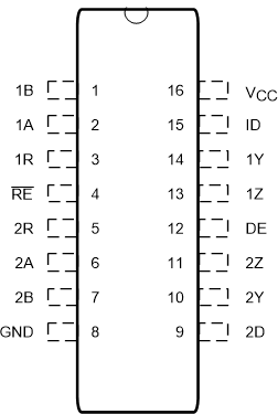
 Figure 4-1 NS or PW Package16 Pin (NS or TSSOP)Top View
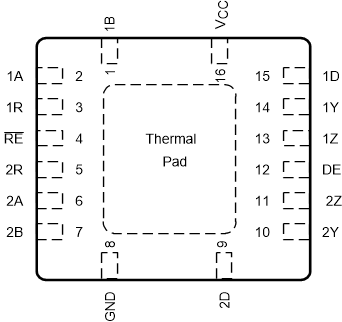
 Figure 4-2 RGY Package16 Pin (VQFN)Top View
Table 4-1 Pin Functions, SN65C1167E
| PIN | I/O | DESCRIPTION | |||
|---|---|---|---|---|---|
| NAME | SO | TSSOP | VQFN | ||
| 1A | 2 | 2 | 2 | I | RS422 differential input (noninverting) to receiver 1 |
| 2A | 6 | 6 | 6 | I | RS422 differential input (noninverting) to receiver 2 |
| 1B | 1 | 1 | 1 | I | RS422 differential input (inverting) to receiver 1 |
| 2B | 7 | 7 | 7 | I | RS422 differential input (inverting) to receiver 2 |
| 1D | 15 | 15 | 15 | I | Logic data input to RS422 driver 1 |
| 2D | 9 | 9 | 9 | I | Logic data input to RS422 driver 2 |
| DE | 12 | 12 | 12 | I | Driver enable (active high) |
| GND | 8 | 8 | 8 | — | Device ground pin |
| 1R | 3 | 3 | 3 | O | Logic data output of RS422 receiver 1 |
| 2R | 5 | 5 | 5 | O | Logic data output of RS422 receiver 2 |
| RE | 4 | 4 | 4 | I | Receiver enable pin (active low) |
| VCC | 16 | 16 | 16 | — | Power supply |
| 1Y | 14 | 14 | 14 | O | RS-422 differential (noninverting) driver output 1 |
| 2Y | 10 | 10 | 10 | O | RS-422 differential (noninverting) driver output 2 |
| 1Z | 13 | 13 | 13 | O | RS-422 differential (inverting) driver output 1 |
| 2Z | 11 | 11 | 11 | O | RS-422 differential (inverting) driver output 2 |
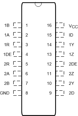
 Figure 4-3 NS or PW Package16 Pin (NS or TSSOP)Top View
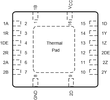
 Figure 4-4 RGY Package16 Pin (VQFN)Top View
Table 4-2 Pin Functions, SN65C1168E
| PIN | I/O | DESCRIPTION | |||
|---|---|---|---|---|---|
| NAME | SO | TSSOP | VQFN | ||
| 1A | 2 | 2 | 2 | I | RS422 differential input (noninverting) to receiver 1 |
| 2A | 6 | 6 | 6 | I | RS422 differential input (noninverting) to receiver 2 |
| 1B | 1 | 1 | 1 | I | RS422 differential input (inverting) to receiver 1 |
| 2B | 7 | 7 | 7 | I | RS422 differential input (inverting) to receiver 2 |
| 1D | 15 | 15 | 15 | I | Logic data input to RS422 driver 1 |
| 2D | 9 | 9 | 9 | I | Logic data input to RS422 driver 2 |
| 1DE | 4 | 4 | 4 | I | Driver 1 enable (active high) |
| 2DE | 12 | 12 | 12 | I | Driver 2 enable (active high) |
| GND | 8 | 8 | 8 | — | Device ground |
| 1R | 3 | 3 | 3 | O | Logic data output of RS422 receiver 1 |
| 2R | 5 | 5 | 5 | O | Logic data output of RS422 receiver 2 |
| VCC | 16 | 16 | 16 | — | Power supply |
| 1Y | 14 | 14 | 14 | O | RS-422 differential (noninverting) driver output 1 |
| 2Y | 10 | 10 | 10 | O | RS-422 differential (noninverting) driver output 2 |
| 1Z | 13 | 13 | 13 | O | RS-422 differential (noninverting) driver output 1 |
| 2Z | 11 | 11 | 11 | O | RS-422 differential (noninverting) driver output 2 |