ZHCSUM3C March 2007 – February 2024 SN65C1167E , SN65C1168E
PRODUCTION DATA
- 1
- 1 特性
- 2 应用
- 3 说明
- 4 Pin Configuration and Functions
-
5 Specifications
- 5.1 Absolute Maximum Ratings
- 5.2 Driver Output and Receiver Input ESD Ratings
- 5.3 Recommended Operating Conditions
- 5.4 Thermal Information
- 5.5 Driver Section Electrical Characteristics
- 5.6 Receiver Section Electrical Characteristics
- 5.7 Driver Section Switching Characteristics
- 5.8 Receiver Section Switching Characteristics
- 6 Parameter Measurement Information
- 7 Detailed Description
- 8 Application and Implementation
- 9 Device and Documentation Support
- 10Revision History
- 11Mechanical, Packaging, and Orderable Information
封装选项
机械数据 (封装 | 引脚)
散热焊盘机械数据 (封装 | 引脚)
- RGY|16
订购信息
6 Parameter Measurement Information
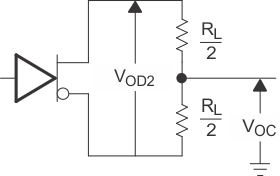
 Figure 6-1 Driver Test Circuit, VOD and VOC
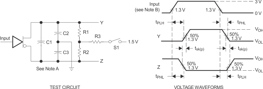
A. C1, C2, and C3 include probe and jig capacitance.
B. The input pulse is supplied by a generator having the following characteristics: PRR = 1 MHz, duty cycle = 50%, tr = tf ≤ 6ns.
Figure 6-2 Driver Test Circuit and Voltage Waveforms
A. C1, C2, and C3 include probe and jig capacitance.
B. The input pulse is supplied by a generator having the following characteristics: PRR = 1 MHz, duty cycle = 50%, tr = tf ≤ 6ns.
Figure 6-3 Driver Test Circuit and Voltage Waveforms
A. C1, C2, and C3 include probe and jig capacitance.
B. The input pulse is supplied by a generator having the following characteristics: PRR = 1 MHz, duty cycle = 50%, tr = tf ≤ 6ns.
Figure 6-4 Driver Test Circuit and Voltage Waveforms
A. C1, C2, and C3 include probe and jig capacitance.
B. The input pulse is supplied by a generator having the following characteristics: PRR = 1 MHz, duty cycle = 50%, tr = tf ≤ 6ns.
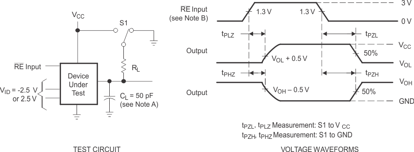
Figure 6-5 Receiver Test Circuit and Voltage Waveforms
A. C1, C2, and C3 include probe and jig capacitance.
B. The input pulse is supplied by a generator having the following characteristics: PRR = 1 MHz, duty cycle = 50%, tr = tf ≤ 6ns.
Figure 6-6 Receiver Test Circuit and Voltage Waveforms