ZHCSK15 July 2019 SN65C1168E-SEP
PRODUCTION DATA.
7 Parameter Measurement Information
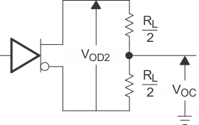
 Figure 1. Driver Test Circuit, VOD and VOC
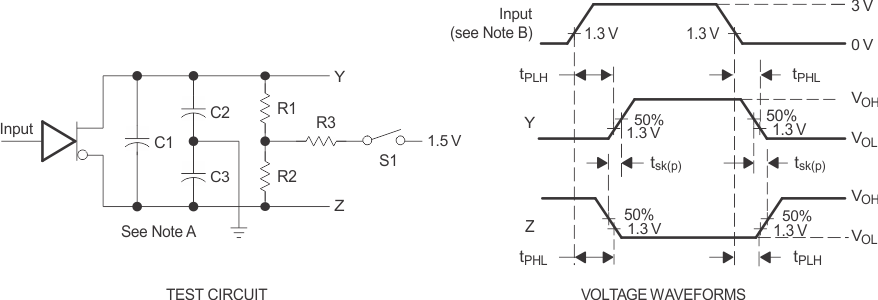
A. C1, C2, and C3 include probe and jig capacitance.
B. The input pulse is supplied by a generator having the following characteristics: PRR = 1 MHz, duty cycle = 50%, tr = tf ≤ 6 ns.
Figure 2. Driver Test Circuit and Voltage Waveforms 
A. C1, C2, and C3 include probe and jig capacitance.
B. The input pulse is supplied by a generator having the following characteristics: PRR = 1 MHz, duty cycle = 50%, tr = tf ≤ 6 ns.
Figure 3. Driver Test Circuit and Voltage Waveforms 
A. C1, C2, and C3 include probe and jig capacitance.
B. The input pulse is supplied by a generator having the following characteristics: PRR = 1 MHz, duty cycle = 50%, tr = tf ≤ 6 ns.
Figure 4. Driver Test Circuit and Voltage Waveforms 
A. C1, C2, and C3 include probe and jig capacitance.
B. The input pulse is supplied by a generator having the following characteristics: PRR = 1 MHz, duty cycle = 50%, tr = tf ≤ 6 ns.
Figure 5. Receiver Test Circuit and Voltage Waveforms 
A. C1, C2, and C3 include probe and jig capacitance.
B. The input pulse is supplied by a generator having the following characteristics: PRR = 1 MHz, duty cycle = 50%, tr = tf ≤ 6 ns.
Figure 6. Receiver Test Circuit and Voltage Waveforms