ZHCSK15 July   2019 SN65C1168E-SEP

PRODUCTION DATA.  

  1. 特性
  2. 应用
  3. 说明
    1.     Device Images
      1.      方框图
  4. 修订历史记录
  5. Pin Configuration and Functions
    1.     Pin Functions
  6. Specifications
    1. 6.1 Absolute Maximum Ratings
    2. 6.2 ESD Ratings
    3. 6.3 Recommended Operating Conditions
    4. 6.4 Thermal Information
    5. 6.5 Driver Section Electrical Characteristics
    6. 6.6 Receiver Section Electrical Characteristics
    7. 6.7 Driver Section Switching Characteristics
    8. 6.8 Receiver Section Switching Characteristics
  7. Parameter Measurement Information
  8. Detailed Description
    1. 8.1 Overview
    2. 8.2 Functional Block Diagram
    3. 8.3 Feature Description
      1. 8.3.1 Active High Driver Output Enables
    4. 8.4 Device Functional Modes
  9. Application and Implementation
    1. 9.1 Application Information
    2. 9.2 Typical Application
      1. 9.2.1 Design Requirements
      2. 9.2.2 Detailed Design Procedure
  10. 10Power Supply Recommendations
  11. 11器件和文档支持
    1. 11.1 器件支持
      1. 11.1.1 第三方米6体育平台手机版_好二三四免责声明
    2. 11.2 接收文档更新通知
    3. 11.3 社区资源
    4. 11.4 商标
    5. 11.5 静电放电警告
    6. 11.6 Glossary
  12. 12机械、封装和可订购信息

封装选项

机械数据 (封装 | 引脚)
散热焊盘机械数据 (封装 | 引脚)
订购信息

Application Information

Figure 7 shows a typical RS-422 application. One transmitter is able to broadcast to multiple receiving nodes connected together over a shared differential bus. Twisted-pair cabling with a controlled differential impedance is used, and a termination resistance is placed at the farthest receive end of the cable in order to match the transmission line impedance and minimize signal reflections.
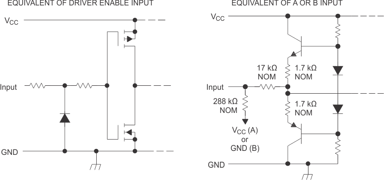
SN65C1168E-SEP schemin_lls740.gifFigure 7. Schematic of Inputs
SN65C1168E-SEP schemout_lls740.gifFigure 8. Schematic of Outputs