ZHCSE15F July 2015 – May 2018 SN65DP159 , SN75DP159
PRODUCTION DATA.
- 1 特性
- 2 应用
- 3 说明
- 4 修订历史记录
- 5 说明 (续)
- 6 Pin Configuration and Functions
-
7 Specifications
- 7.1 Absolute Maximum Ratings
- 7.2 ESD Ratings
- 7.3 Recommended Operating Conditions
- 7.4 Thermal Information
- 7.5 Power Supply Electrical Characteristics
- 7.6 Differential Input Electrical Characteristics
- 7.7 HDMI and DVI TMDS Output Electrical Characteristics
- 7.8 AUX, DDC, and I2C Electrical Characteristics
- 7.9 HPD Electrical Characteristics
- 7.10 HDMI and DVI Main Link Switching Characteristics
- 7.11 AUX Switching Characteristics (Only for RGZ Package)
- 7.12 HPD Switching Characteristics
- 7.13 DDC and I2C Switching Characteristics
- 7.14 Typical Characteristics
- 8 Parameter Measurement Information
-
9 Detailed Description
- 9.1 Overview
- 9.2 Functional Block Diagram
- 9.3
Feature Description
- 9.3.1 Reset Implementation
- 9.3.2 Operation Timing
- 9.3.3 I2C-over-AUX to DDC Bridge (SNx5DP159 48-Pin Package Version Only)
- 9.3.4 Input Lane Swap and Polarity Working
- 9.3.5 Main Link Inputs
- 9.3.6 Main Link Inputs Debug Tools
- 9.3.7 Receiver Equalizer
- 9.3.8 Termination Impedance Control
- 9.3.9 TMDS Outputs
- 9.4 Device Functional Modes
- 9.5 Register Maps
- 10Application and Implementation
- 11Power Supply Recommendations
- 12Layout
- 13器件和文档支持
- 14机械、封装和可订购信息
封装选项
机械数据 (封装 | 引脚)
散热焊盘机械数据 (封装 | 引脚)
订购信息
12.1 Layout Guidelines
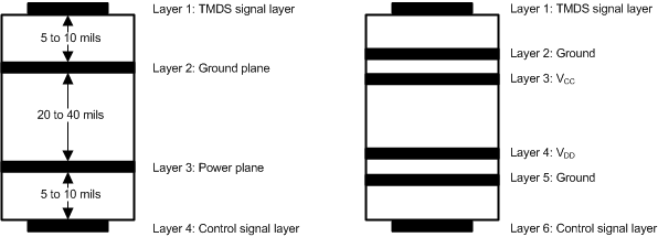
TI recommends to use at a minimum a four layer stack up to accomplish a low-EMI PCB design. TI recommends six layers because the SNx5DP159 is a two voltage rail device.
- Routing the high-speed input DisplayPort traces and TMDS output traces on the top layer avoids the use of vias (and their discontinuities) and allows for clean interconnects from the HDMI connectors to the repeater inputs and from the repeater output to the subsequent receiver circuit. It is important to match the electrical length of these high speed traces to minimize both inter-pair and intra-pair skew.
- Placing a solid ground plane next to the high-speed signal layer establishes controlled impedance for transmission line interconnects and provides an excellent low-inductance path for the return current flow.
- Placing the power plane next to the ground plane creates additional high-frequency bypass capacitance.
- Routing the slower speed control signals on the bottom layer allows for greater flexibility as these signal links usually have margin to tolerate discontinuities such as vias.
- If an additional supply voltage plane or signal layer is needed, add a second power / ground plane system to the stack to keep it symmetrical. This makes the stack mechanically stable and prevents it from warping. Also the power and ground plane of each power system can be placed closer together, thus increasing the high- frequency bypass capacitance significantly.
- The control pin pullup and pulldown resistors are shown in application section for reference. If a high is needed only use the pull up. If a low is needed only use the pull down. If mid level is to be selected do not use either resistors and leave the pin floating/No connect.
 Figure 35. Recommended 4- or 6-Layer Stack for a Receiver PCB Design