ZHCSFS1A December   2016  – June 2018 SN65DSI84-Q1

PRODUCTION DATA.  

  1. 特性
  2. 应用
  3. 说明
    1. 3.1 典型应用
  4. 修订历史记录
  5. Pin Configuration and Functions
    1.     Pin Functions
  6. Specifications
    1. 6.1 Absolute Maximum Ratings
    2. 6.2 ESD Ratings
    3. 6.3 Recommended Operating Conditions
    4. 6.4 Thermal Information
    5. 6.5 Electrical Characteristics
    6. 6.6 Switching Characteristics
  7. Parameter Measurement Information
  8. Detailed Description
    1. 8.1 Overview
    2. 8.2 Functional Block Diagram
    3. 8.3 Feature Description
      1. 8.3.1 Clock Configurations and Multipliers
      2. 8.3.2 ULPS
      3. 8.3.3 LVDS Pattern Generation
    4. 8.4 Device Functional Modes
      1. 8.4.1 Reset Implementation
      2. 8.4.2 Initialization Sequence
      3. 8.4.3 LVDS Output Formats
      4. 8.4.4 DSI Lane Merging
      5. 8.4.5 DSI Pixel Stream Packets
      6. 8.4.6 DSI Video Transmission Specifications
      7. 8.4.7 Operating Modes
    5. 8.5 Programming
      1. 8.5.1 Local I2C Interface Overview
    6. 8.6 Register Maps
      1. 8.6.1 Control and Status Registers Overview
        1. 8.6.1.1 CSR Bit Field Definitions – ID Registers
          1. 8.6.1.1.1 Registers 0x00 – 0x08
            1. Table 5. Registers 0x00 – 0x08 Field Descriptions
        2. 8.6.1.2 CSR Bit Field Definitions – Reset and Clock Registers
          1. 8.6.1.2.1 Register 0x09
            1. Table 6. Register 0x09 Field Descriptions
          2. 8.6.1.2.2 Register 0x0A
            1. Table 7. Register 0x0A Field Descriptions
          3. 8.6.1.2.3 Register 0x0B
            1. Table 8. Register 0x0B Field Descriptions
          4. 8.6.1.2.4 Register 0x0D
            1. Table 9. Register 0x0D Field Descriptions
        3. 8.6.1.3 CSR Bit Field Definitions – DSI Registers
          1. 8.6.1.3.1 Register 0x10
            1. Table 10. Register 0x10 Field Descriptions
          2. 8.6.1.3.2 Register 0x11
            1. Table 11. Register 0x11 Field Descriptions
          3. 8.6.1.3.3 Register 0x12
            1. Table 12. Register 0x12 Field Descriptions
        4. 8.6.1.4 CSR Bit Field Definitions – LVDS Registers
          1. 8.6.1.4.1 Register 0x18
            1. Table 13. Register 0x18 Field Descriptions
          2. 8.6.1.4.2 Register 0x19
            1. Table 14. Register 0x19 Field Descriptions
          3. 8.6.1.4.3 Register 0x1A
            1. Table 15. Register 0x1A Field Descriptions
          4. 8.6.1.4.4 Register 0x1B
            1. Table 16. Register 0x1B Field Descriptions
        5. 8.6.1.5 CSR Bit Field Definitions – Video Registers
          1. 8.6.1.5.1  Register 0x20
            1. Table 17. Register 0x20 Field Descriptions
          2. 8.6.1.5.2  Register 0x21
            1. Table 18. Register 0x21 Field Descriptions
          3. 8.6.1.5.3  Register 0x24
            1. Table 19. Register 0x24 Field Descriptions
          4. 8.6.1.5.4  Register 0x25
            1. Table 20. Register 0x25 Field Descriptions
          5. 8.6.1.5.5  Register 0x28
            1. Table 21. Register 0x28 Field Descriptions
          6. 8.6.1.5.6  Register 0x29
            1. Table 22. Register 0x29 Field Descriptions
          7. 8.6.1.5.7  Register 0x2C
            1. Table 23. Register 0x2C Field Descriptions
          8. 8.6.1.5.8  Register 0x2D
            1. Table 24. Register 0x2D Field Descriptions
          9. 8.6.1.5.9  Register 0x30
            1. Table 25. Register 0x30 Field Descriptions
          10. 8.6.1.5.10 Register 0x31
            1. Table 26. Register 0x31 Field Descriptions
          11. 8.6.1.5.11 Register 0x34
            1. Table 27. Register 0x34 Field Descriptions
          12. 8.6.1.5.12 Register 0x36
            1. Table 28. Register 0x36 Field Descriptions
          13. 8.6.1.5.13 Register 0x38
            1. Table 29. Register 0x38 Field Descriptions
          14. 8.6.1.5.14 Register 0x3A
            1. Table 30. Register 0x3A Field Descriptions
          15. 8.6.1.5.15 Register 0x3C
            1. Table 31. Register 0x3C Field Descriptions
        6. 8.6.1.6 CSR Bit Field Definitions – IRQ Registers
          1. 8.6.1.6.1 Register 0xE0
            1. Table 32. Register 0xE0 Field Descriptions
          2. 8.6.1.6.2 Register 0xE1
            1. Table 33. Register 0xE1 Field Descriptions
          3. 8.6.1.6.3 Register 0xE5
            1. Table 34. Register 0xE5 Field Descriptions
  9. Application and Implementation
    1. 9.1 Application Information
      1. 9.1.1 Video Stop and Restart Sequence
      2. 9.1.2 Reverse LVDS Pin Order Option
      3. 9.1.3 IRQ Usage
    2. 9.2 Typical Application
      1. 9.2.1 Design Requirements
      2. 9.2.2 Detailed Design Procedure
        1. 9.2.2.1 Example Script
      3. 9.2.3 Application Curve
  10. 10Power Supply Recommendations
    1. 10.1 VCC Power Supply
    2. 10.2 VCORE Power Supply
  11. 11Layout
    1. 11.1 Layout Guidelines
      1. 11.1.1 Package Specific
      2. 11.1.2 Differential Pairs
      3. 11.1.3 Ground
    2. 11.2 Layout Example
  12. 12器件和文档支持
    1. 12.1 文档支持
      1. 12.1.1 相关文档
    2. 12.2 接收文档更新通知
    3. 12.3 社区资源
    4. 12.4 商标
    5. 12.5 静电放电警告
    6. 12.6 术语表
  13. 13机械、封装和可订购信息

封装选项

机械数据 (封装 | 引脚)
散热焊盘机械数据 (封装 | 引脚)
订购信息

LVDS Output Formats

The SN65DSI84-Q1 processes DSI packets and produces video data driven to the LVDS interface in an industry standard format. Single-Link LVDS and Dual-Link LVDS are supported by the SN65DSI84-Q1; when the LVDS output is implemented in a Dual-Link configuration, channel A carries the odd pixel data, and channel B carries the even pixel data. During conditions such as the default condition, and some video synchronization periods, where no video stream data is passing from the DSI input to the LVDS output, the SN65DSI84-Q1 transmits zero value pixel data on the LVDS outputs while maintaining transmission of the vertical sync and horizontal sync status.

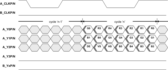
Figure 8 illustrates a Single-Link LVDS 18bpp application.

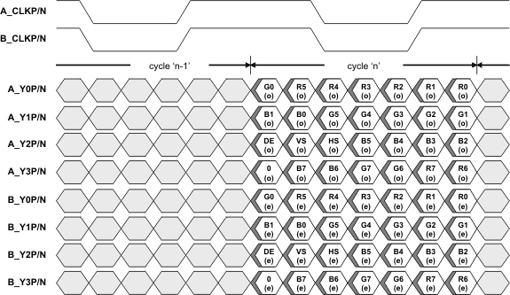
Figure 9 illustrates a Dual-Link 24 bpp application using Format 2, controlled by CHA_24BPP_FORMAT1 (CSR 0x18.1) and CHB_24BPP_FORMAT1 (CSR 0x18.0). In data Format 2, the two MSB per color are transferred on the Y3P/N LVDS lane.

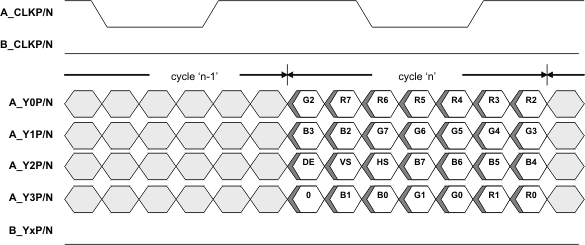
Figure 10 illustrates a 24 bpp Single-Link application using Format 1. In data Format 1, the two LSB per color are transferred on the Y3P/N LVDS lane.

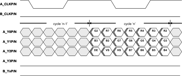
Figure 11 illustrates a Single-Link LVDS application where 24 bpp data is received from DSI and converted to 18 bpp data for transmission to an 18 bpp panel. This application is configured by setting CHA_24BPP_FORMAT1 (CSR 0x18.1) to ‘1’ and CHA_24BPP_MODE (CSR 0x18.3) to ‘0’. In this configuration, the SN65DSI84-Q1 will not transmit the 2 LSB per color because the Y3P/N LVDS lane is disabled.

NOTE

Note: Figure 8, Figure 9, Figure 10, and Figure 11 only illustrate a few example applications for the SN65DSI84-Q1. Other applications are also supported.
SN65DSI84-Q1 fig4_flatlink_LLSEB9.gif
DE = Data Enable; Channel B Clock, Channel B Data, and A_Y3P/N are Output Low
Figure 8. LVDS Output Data; Single-Link 18 Bpp
SN65DSI84-Q1 fig5_flatlink_LLSEB9.gif
DE = Data Enable; (o) = Odd Pixels; (e) = Even Pixels
Figure 9. LVDS Output Data (Format 2); Dual-Link 24 Bpp
SN65DSI84-Q1 fig6_flatlink_LLSEB9.gif
DE = Data Enable; Channel B Clock and Data are Output Low
Figure 10. LVDS Output Data (Format 1); Single-Link 24 Bpp
SN65DSI84-Q1 fig7_flatlink_LLSEB9.gif
DE = Data Enable; Channel B Clock, Channel B Data, and A_Y3P/N a re Output Low; Channel B Clock, Channel B Data, and A_Y3P/N are Output Low
Figure 11. LVDS Output Data (Format 1); 24-Bpp to Single-Link 18-Bpp Conversion