ZHCSAU2G September   2012  – June 2018 SN65DSI84

PRODUCTION DATA.  

  1. 特性
  2. 应用
  3. 说明
    1.     典型应用
  4. 修订历史记录
  5. Pin Configuration and Functions
    1.     Pin Functions
  6. Specifications
    1. 6.1 Absolute Maximum Ratings
    2. 6.2 EDS Ratings
    3. 6.3 Recommended Operating Conditions
    4. 6.4 Thermal Information
    5. 6.5 Electrical Characteristics
    6. 6.6 Switching Characteristics
  7. Detailed Description
    1. 7.1 Overview
    2. 7.2 Functional Block Diagram
    3. 7.3 Feature Description
      1. 7.3.1 Clock Configurations and Multipliers
      2. 7.3.2 ULPS
      3. 7.3.3 LVDS Pattern Generation
    4. 7.4 Device Functional Modes
      1. 7.4.1 Reset Implementation
      2. 7.4.2 Initialization Sequence
      3. 7.4.3 LVDS Output Formats
      4. 7.4.4 DSI Lane Merging
      5. 7.4.5 DSI Pixel Stream Packets
      6. 7.4.6 DSI Video Transmission Specifications
      7. 7.4.7 Operating Modes
    5. 7.5 Programming
      1. 7.5.1 Local I2C Interface Overview
    6. 7.6 Register Maps
      1. 7.6.1 Control and Status Registers Overview
  8. Application and Implementation
    1. 8.1 Application Information
      1. 8.1.1 Video Stop and Restart Sequence
      2. 8.1.2 Reverse LVDS Pin Order Option
      3. 8.1.3 IRQ Usage
    2. 8.2 Typical Application
      1. 8.2.1 Design Requirements
      2. 8.2.2 Detailed Design Procedure
        1. 8.2.2.1 Example Script
      3. 8.2.3 Application Curve
  9. Power Supply Recommendations
    1. 9.1 VCC Power Supply
    2. 9.2 VCORE Power Supply
  10. 10Layout
    1. 10.1 Layout Guidelines
      1. 10.1.1 Package Specific
      2. 10.1.2 Differential Pairs
      3. 10.1.3 Ground
    2. 10.2 Layout Example
  11. 11器件和文档支持
    1. 11.1 接收文档更新通知
    2. 11.2 社区资源
    3. 11.3 商标
    4. 11.4 静电放电警告
    5. 11.5 术语表
  12. 12机械、封装和可订购信息

封装选项

机械数据 (封装 | 引脚)
散热焊盘机械数据 (封装 | 引脚)
订购信息

Reset Implementation

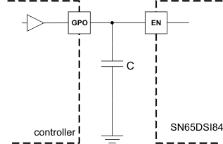
When EN is de-asserted (low), the SN65DSI84 is in SHUTDOWN or RESET state. In this state, CMOS inputs are ignored, the MIPI® D-PHY inputs are disabled and outputs are high impedance. It is critical to transition the EN input from a low to a high level after the VCC supply has reached the minimum operating voltage as shown in Figure 6. This is achieved by a control signal to the EN input, or by an external capacitor connected between EN and GND.
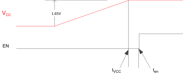
SN65DSI84 cold_start_Vcc_LLSEB9.gifFigure 6. Cold Start VCC Ramp up to EN

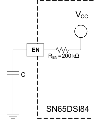
When implementing the external capacitor, the size of the external capacitor depends on the power up ramp of the VCC supply, where a slower ramp-up results in a larger value external capacitor. See the latest reference schematic for the SN65DSI84 device and, or consider approximately 200 nF capacitor as a reasonable first estimate for the size of the external capacitor.

Both EN implementations are shown in Figure 7 and Figure 8.
SN65DSI84 external_cap_controller_LLSEC2.gif
Figure 7. External Capacitor Controlled EN
SN65DSI84 EN_input_from_active_controller_LLSEC2.gif
Figure 8. EN Input From Active Controller

When the SN65DSI84 is reset while VCC is high, the EN pin must be held low for at least 10 ms before being asserted high as described in Table 2 to be sure that the device is properly reset. The DSI CLK lane MUST be in HS and the DSI data lanes MUST be driven to LP11 while the device is in reset before the EN pin is asserted per the timing described in Table 2.